

Method for realizing site programmeable gate array loading
A gate array and control register technology, applied in program loading/starting, program control devices, instruments, etc., can solve the problems of reducing loading rate, long loading time, increasing cost, etc., and achieve the effect of reducing the number of visits and increasing the loading rate
- Summary
- Abstract
- Description
- Claims
- Application Information
AI Technical Summary
Problems solved by technology
Method used
Image

Examples
Embodiment Construction
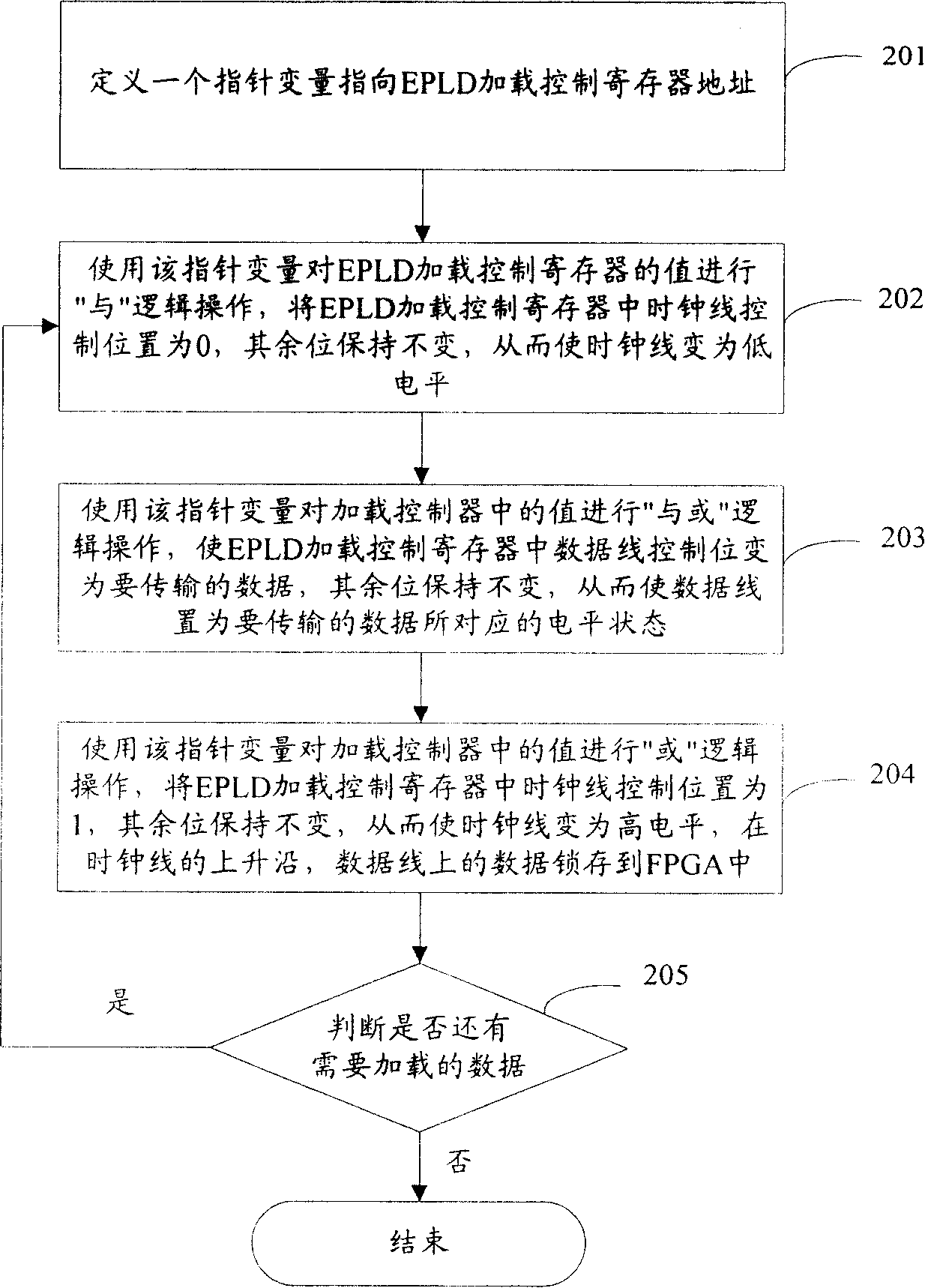
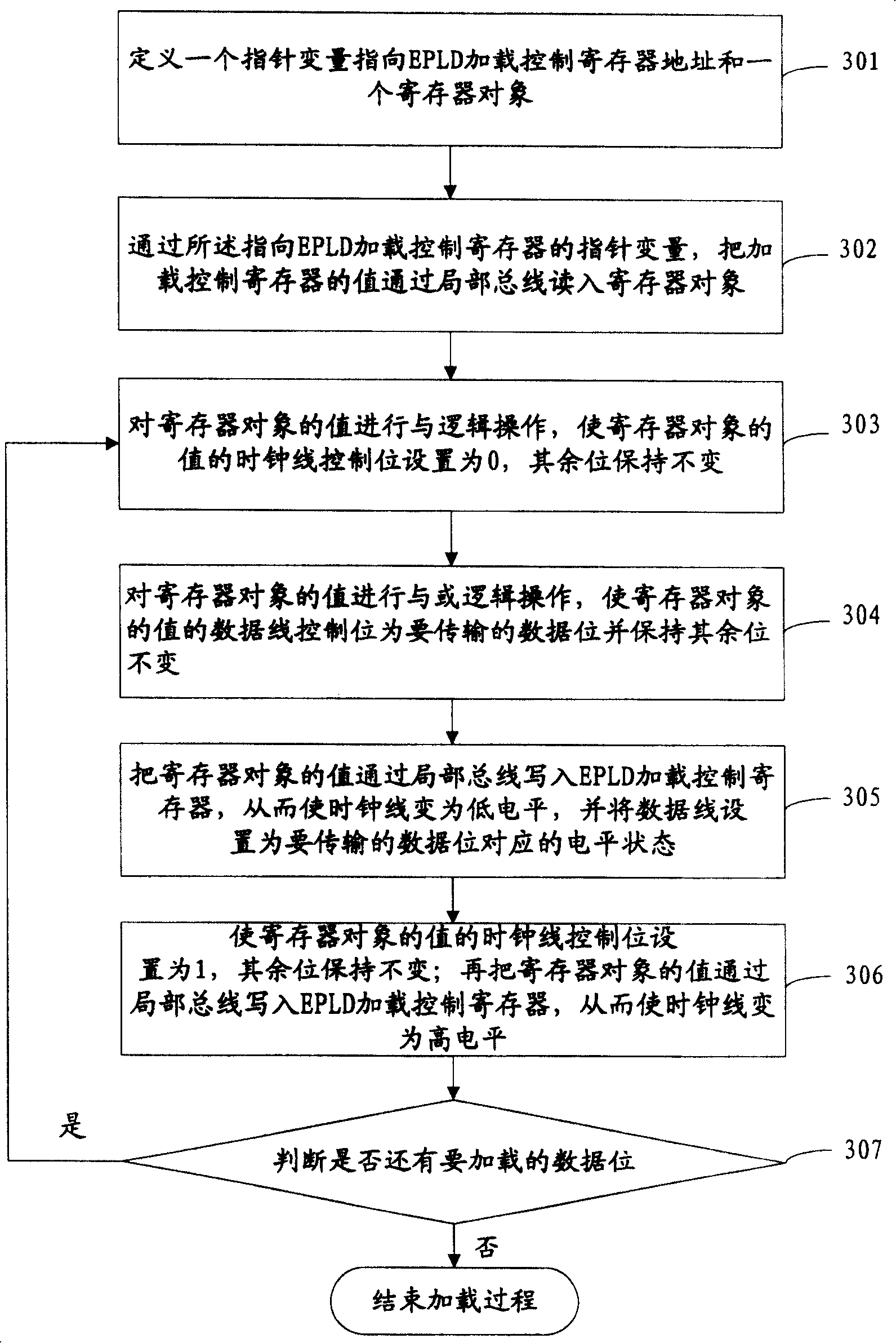
[0038] In order to make the purpose, technical solution and advantages of the present invention clearer, the present invention will be further elaborated below in conjunction with the accompanying drawings.
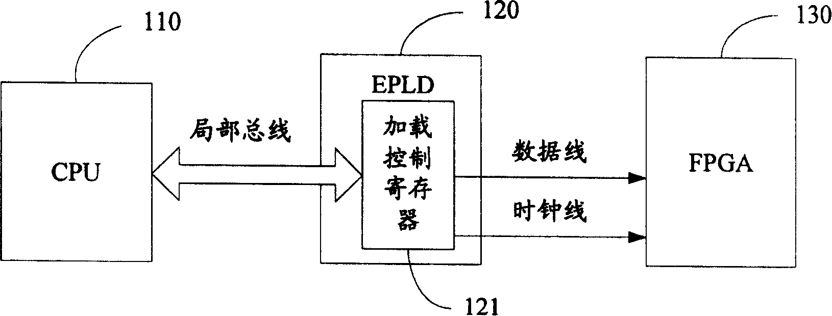
[0039]The core content of the present invention is: define a register object, first read the value in the EPLD loading control register and store in this object; The bus is written into the EPLD load control register, so that each time a data is loaded, the number of visits to the EPLD load control register is reduced to two; in addition, according to the specific regulations of the chip, the FPGA only latches the data on the rising or falling edge of the clock line , so the data line can be set at the same time on the falling edge or rising edge of the clock line, ready to transmit the next data, which can further save the time required for loading and increase the loading speed. In the following, for the convenience of description, the clock edge where the FPGA latches ...
PUM
 Abstract
Description
Claims
Application Information