Stacked photoelectric converter

A conversion device, photoelectric technology, applied in the direction of photovoltaic power generation, circuits, electrical components, etc., can solve the problems of increased production cost and time, increased area loss of photoelectric conversion area, interface pollution, etc., to avoid the reduction of photoelectric conversion efficiency, reduce Effects on production cost and time

Inactive Publication Date: 2008-09-17
KANEKA CORP
View PDF11 Cites 4 Cited by
  • Summary
  • Abstract
  • Description
  • Claims
  • Application Information

AI Technical Summary

Problems solved by technology

[0032] In addition, when an integrated thin-film photoelectric conversion module is manufactured using a TCO layer in the intermediate reflection layer, in the structure having the first separation groove, the second separation groove, and the connection groove, leakage current is generated, and the characteristics of the photoelectric conversion module are deteriorated. question
[0033] The leakage current issues such as Figure 32 As shown, it can be solved by arranging the third separation groove 124, but since the patterning will be added once, the problem of production cost and time increase will occur.
In addition, the interface between the middle reflection layer and the rear photoelectric conversion module may be polluted due to exposure to the atmosphere
In addition, due to the provision of the third separation groove, there will be a problem that the area loss of the effective photoelectric conversion region will increase.

Method used


Image

  • Stacked photoelectric converter
  • Stacked photoelectric converter
  • Stacked photoelectric converter

Examples


Embodiment 1

[0185] As Example 1, manufactured Figure 10 The stacked photoelectric conversion device shown. The device of this embodiment 1 is only in the point that the n-type silicon compound layer 4 with a thickness of 30 nm is formed between the front photoelectric conversion unit 3 and the wide photoelectric conversion unit 5 and Figure 15 The device of Comparative Example 1 shown is different. In addition, the n-type silicon composite layer 4 can also be considered as a part of the n-type layer included in the front photoelectric conversion unit 3 .

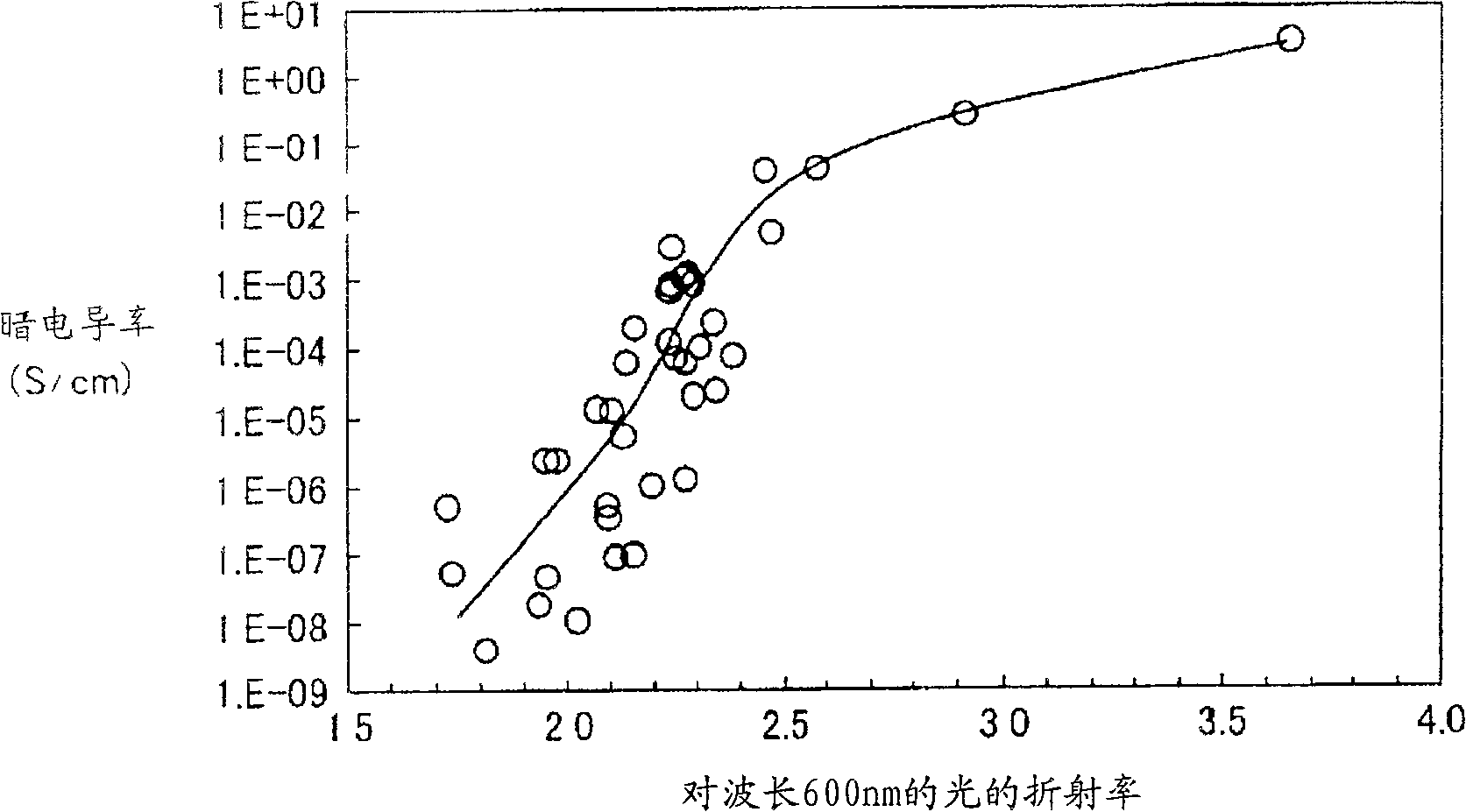
[0186] The film-forming condition of n-type silicon composite layer 4 is that the gas flow ratio is SiH 4 / CO 2 / PH 3 / H 2 =5 / 10 / 0.1 / 1000sccm, power frequency is 13.56MHz, power density is 100mW / cm 2 , the pressure is 100Pa, and the substrate temperature is 200°C. In the formed n-type silicon composite layer 4, the oxygen concentration is 42 atomic%, the optical gap is 2.37eV, the Exps measured by XPS is 3.5eV, the refractive i...

Embodiment 2

[0189] As Example 2, manufactured Figure 17 The stacked photoelectric conversion device shown. The device of this embodiment 2 is only compatible with the n-type layer of the front photoelectric conversion unit 3 by using the n-type silicon composite layer 4 with a thickness of 30 nm as the intermediate reflection layer and the n-type layer. Figure 10 The apparatus of Example 1 is shown differently.

[0190] It can be seen from Table 1 that compared with Example 1, the Jsc of the present embodiment 2 is further increased, the Eff is increased, and the spectrally induced currents of both the front photoelectric conversion unit and the rear photoelectric conversion unit are also increased. This is because the light reflected on the side of the front photoelectric conversion unit 3 and the light transmitted through the side of the rear conversion unit 5 need not all pass through the n-type layer of the front photoelectric conversion unit 3 by the silicon composite layer 4. Ty...

Embodiment 3

[0194] As Example 3, manufactured Figure 18 The stacked photoelectric conversion device shown. In the device of Example 3, only the n-type silicon composite layer 34 with a thickness of 30 nm as the first n-type layer and the n-type microcrystalline silicon layer 35 with a thickness of 5 nm as the second n-type layer are laminated to form the front photoelectric conversion unit. 3 n-type layers at this point and Figure 17 The apparatus of Example 2 is shown differently. Of course, the n-type silicon composite layer 34 of the third embodiment is also formed under the same plasma CVD conditions as the n-type silicon composite layer 4 of the first and second embodiments.

[0195] As can be seen from Table 1, compared with Example 2, the present embodiment 3, although Jsc decreases slightly, FF increases, and Eff increases. In addition, although the spectrally induced current of the front photoelectric conversion unit in Example 3 is slightly lower than that of Example 2, it ...


PUM


Abstract

A stacked photoelectric converter comprising a plurality of stacked photoelectric conversion units (3;5) each including one conductivity type layer (31;51), a photoelectric converting layer (32;52) of substantially intrinsic semiconductor, and a reverse conductivity type layer (33;53) that are formed on a substrate (1) sequentially from the light incident side. At least one of the reverse conductivity type layer (33) in the front photoelectric conversion unit (3) arranged relatively on the light incident side and the one conductivity type layer (51) in the rear photoelectric conversion unit (5) arranged contiguously to the front photoelectric conversion unit (3) includes a silicon composite layer (4). The silicon composite layer (4) has a thickness of 20-130 nm and an oxygen concentration of 25-60 atm%.

Description

technical field [0001] The present invention relates to improvement of conversion efficiency of a thin-film photoelectric conversion device, and in particular to improvement of conversion efficiency of a laminated thin-film photoelectric conversion device in which a plurality of photoelectric conversion units are stacked. In addition, the terms "crystalline" and "fine crystal" in the specification of the present application are also used in the case where an amorphous substance is partially contained, as used in the art. Background technique [0002] In recent years, attention has been paid to thin-film photoelectric conversion devices, which have little problem from the viewpoint of resources, in order to simultaneously achieve both cost reduction and high efficiency of photoelectric conversion devices, and development thereof has been vigorously pursued. Thin-film photoelectric conversion devices are expected to be used in various applications such as solar cells, optical ...

Claims


Application Information

Patent Timeline
Patent Type & Authority Patents(China)
IPC IPC(8): H01L31/075H01L31/04H01L31/0465H01L31/06H01L31/076H01L31/077
CPCY02E10/52Y02E10/547Y02E10/548
Inventor 佐佐木敏明小井洋平山本宪治吉见雅士市川满
Owner KANEKA CORP
Why Eureka
Try Eureka