Supercharge Your Innovation With Domain-Expert AI Agents!

Variable gain control circuit and integrated circuit device having the same

A technology of gain control circuit and integrated circuit, which is applied in the direction of gain control, control amplifier parts, electric solid-state devices, etc., and can solve problems such as large space, high current power consumption and parasitic effects

Inactive Publication Date: 2008-10-22
SAMSUNG ELECTRONICS CO LTD
View PDF4 Cites 0 Cited by
  • Summary
  • Abstract
  • Description
  • Claims
  • Application Information

AI Technical Summary

Problems solved by technology

Therefore, the integrated circuit device equipped with the variable gain control circuit 101 needs more space, has higher current consumption and parasitic effects

Method used


Image

  • Variable gain control circuit and integrated circuit device having the same
  • Variable gain control circuit and integrated circuit device having the same
  • Variable gain control circuit and integrated circuit device having the same

Examples


Embodiment Construction

[0020] Preferred embodiments of the present invention will now be described in more detail with reference to the accompanying drawings. The same reference numerals in different figures represent the same components.

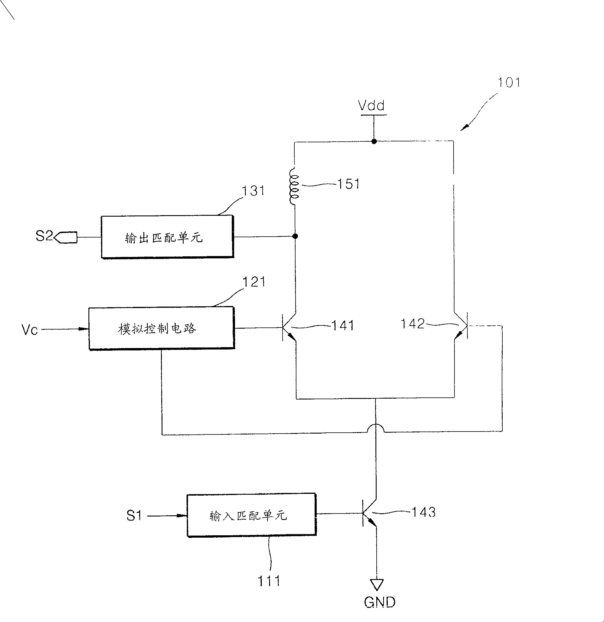
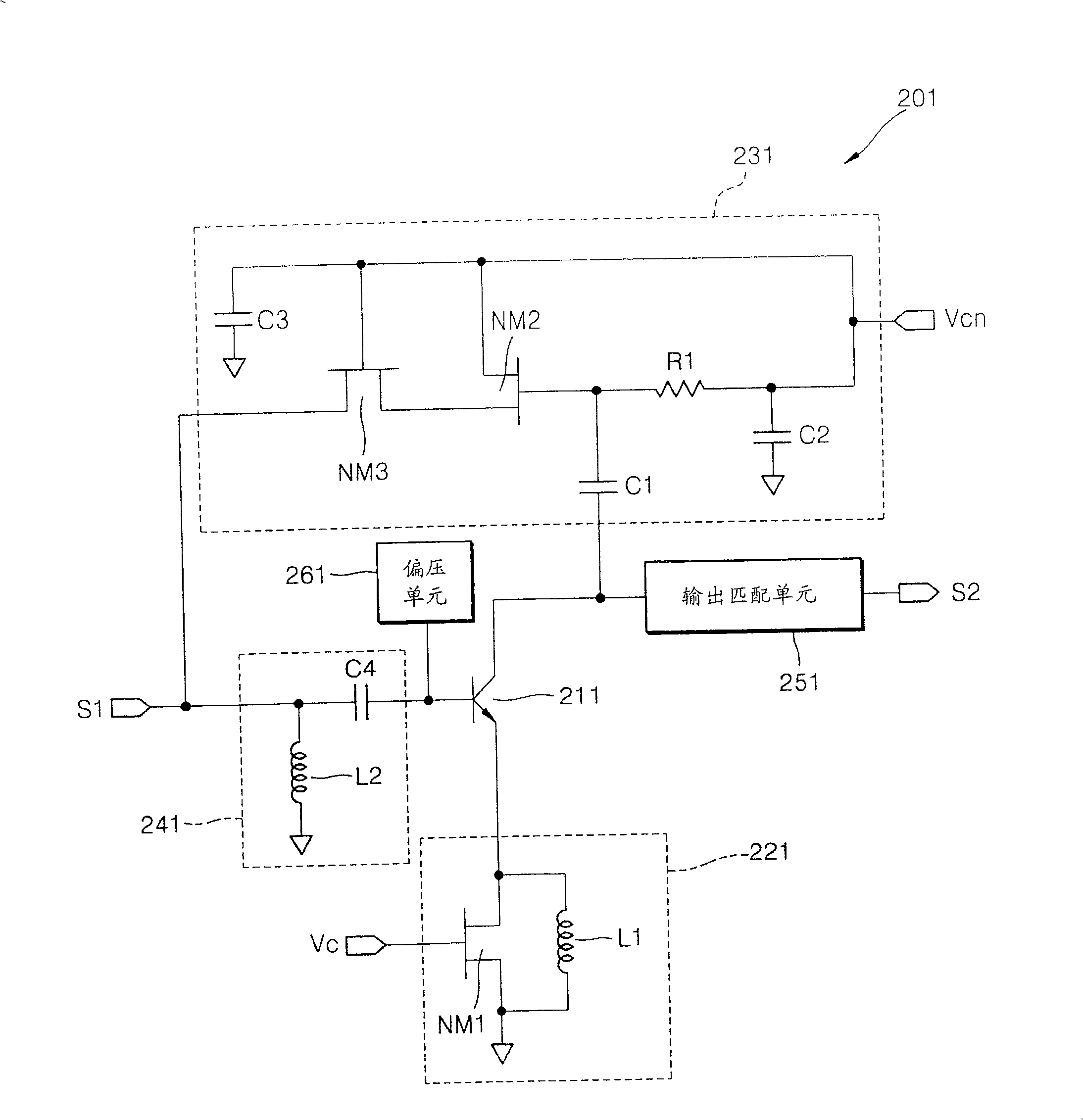
[0021] figure 2 is a circuit diagram of a variable gain control circuit according to a preferred embodiment of the present invention. refer to figure 2 , the variable gain control circuit 201 includes a bipolar transistor 211 , a serial switching unit 221 , a parallel switching unit 231 , an input matching unit 241 , an output matching unit 251 and a bias voltage unit 261 .

[0022] The bipolar transistor 211 amplifies the external input signal S1 applied to the base, and outputs an output signal S2 at the collector thereof. The input signal S1 and the output signal S2 are high-frequency signals. The bipolar transistor 211 is an NPN type transistor.

[0023] The serial switching unit 221 is connected between the emitter of the bipolar transistor 211 and th...


PUM


Abstract

A variable gain control circuit is provided comprising a bipolar transistor for amplifying an input signal applied to a base, and outputs an output signal via a collector; a serial exchanging unit connected between an emitter of the bipolar transistor; a first voltage node; a parallel exchanging unit connected between the collector of the bipolar transistor and the first voltage node, and wherein the gain of the variable gain control circuit increases in a high gain mode by activating the serial exchanging unit and deactivating the parallel exchanging unit, and the gain of the variable gain control circuit decreases in a low gain mode by deactivating the serial exchanging unit and activating the parallel exchanging unit.

Description

technical field [0001] The present invention relates to a variable gain control circuit, and more particularly to a variable gain control circuit embedded in an integrated circuit device. Background technique [0002] Variable gain control circuits are used to control the amount of transmission output gain depending on distance or other communication circumstances, particularly when transmitting signals and transmitting or receiving waves between a mobile communication terminal and a base station. Control of output gain improves power efficiency and prevents unnecessary current leakage into adjacent channels. [0003] figure 1 is the circuit diagram of a conventional variable gain control circuit. refer to figure 1 , the conventional variable gain control circuit includes an input matching circuit 111 , an analog control circuit 121 , an output matching unit 131 , bipolar transistors 141 - 143 and an inductor 151 . [0004] Similar to a differential amplifier, current fl...

Claims


Application Information

Patent Timeline
Patent Type & Authority Patents(China)
IPC IPC(8): H03G3/00H01L27/00H03G3/20H03G1/00
CPCH03G1/0023H03G3/20
Inventor 安圹昊
Owner SAMSUNG ELECTRONICS CO LTD
Features
  • R&D
  • Intellectual Property
  • Life Sciences
  • Materials
  • Tech Scout
  • Unparalleled Data Quality
  • Higher Quality Content
  • 60% Fewer Hallucinations
Learn More