
Patsnap Eureka
For R&D, Patsnap Eureka makes reading and utilizing patents & technical documents easy.
Patsnap Eureka AIR
Designed for self-driven R&D workflows. Generate viable solutions, solve complex R&D challenges, empower your innovation with AI.

Patsnap Eureka Materials
Designed for material experts only. Revolutionize your material R&D, from search, analyze, to developing new materials.

TechResearch
Generate reliable direction feasibility study reports for your R&D in just a few steps.

TechSeek
Discover and master advanced knowledge NOW. Basics, ideas, possibilities, all at once.

TechMind
As an expert in R&D Theories, TechMind can generates customized viable solutions instantly.

TechRisk
Analyze your overall solution with one click, know your potential R&D risks in advance.

TechMonitor
Get weekly tech updates, stay abreast of the latest tech innovations and key insights.
Semiconductor device
A semiconductor, outstanding technology, applied in the direction of semiconductor devices, semiconductor/solid-state device components, electric solid-state devices, etc., can solve the problem of low layout freedom, and achieve the effect of easy assembly and processing
- Summary
- Abstract
- Description
- Claims
- Application Information
AI Technical Summary
Problems solved by technology
Method used
Image

Examples
Embodiment 2
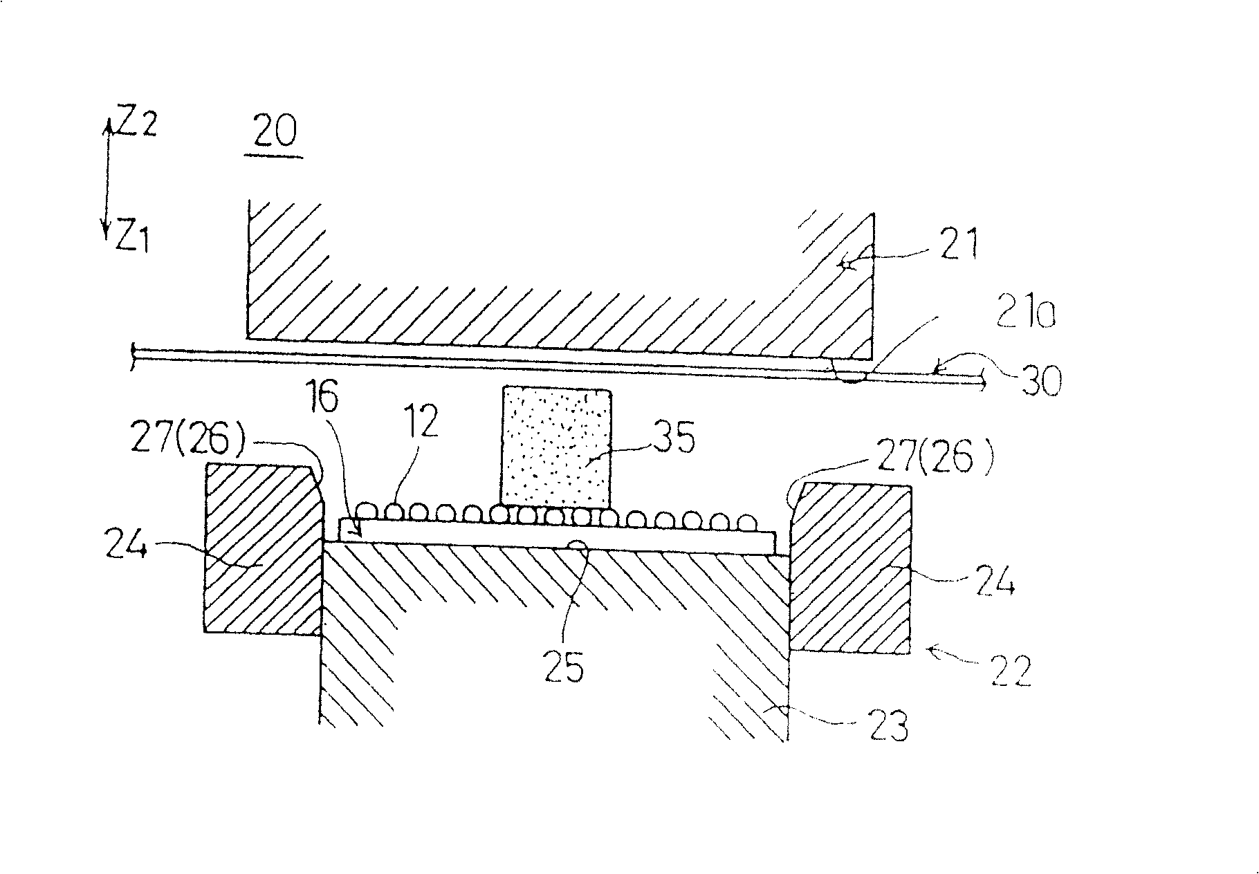
[0356] The semiconductor device 10A of the second embodiment is configured by mounting a plurality of semiconductor devices 11 on a stage member 80 to form a modular structure. In addition, the resin layer 13 is configured to seal the protruding electrode 12 up to the side of the semiconductor device 11 while leaving the tip portion sealed. In addition, the stage 80 is formed of a material (for example, copper or aluminum) with good heat dissipation.
[0357] In the semiconductor device 10A configured as described above, since a material with good heat dissipation is used as the stage 80 , high heat dissipation can be maintained even when a plurality of semiconductor devices 11 are mounted.
[0358] Furthermore, the semiconductor device 10B of Embodiment 3 is characterized in that: Figure 26 In the semiconductor device 10A, the bank portion 81 is formed on the outer peripheral side of the stage 80 . The height H2 ( Figure 27 , indicated by an arrow) is configured to be hi...
Embodiment 9
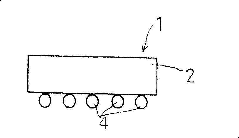
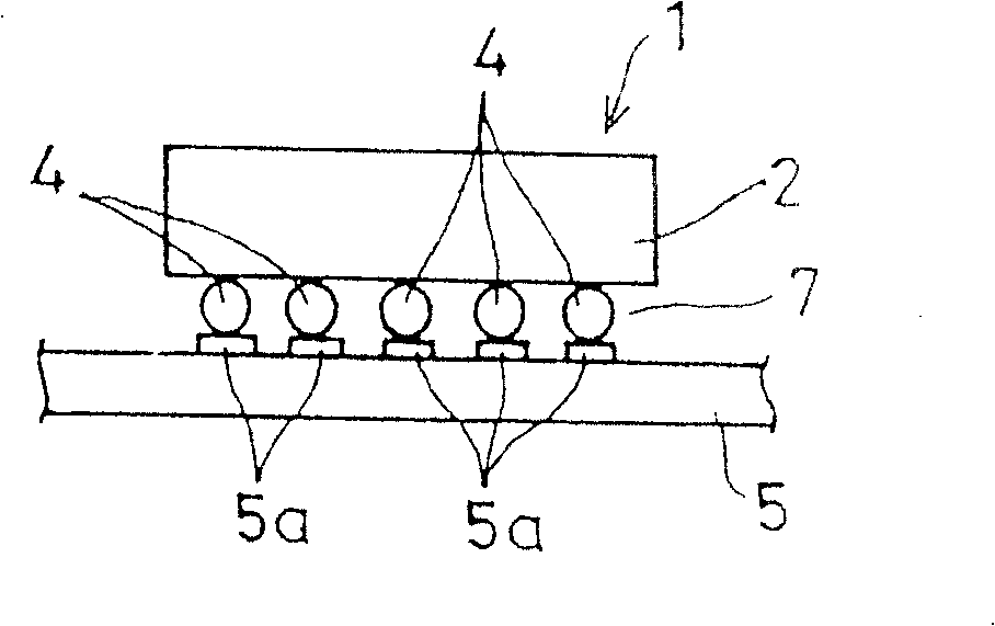
[0368] Figure 29 is an explanatory diagram for explaining the semiconductor manufacturing method of Embodiment 9, in Figure 29 in, for use with Figure 1 to Figure 9 The same configurations as those of the embodiments described in Embodiment 1 are given the same reference numerals and description thereof will be omitted.
[0369] In this embodiment, although it is the same as the above-mentioned embodiment, it is also characterized in that as the sealing resin used in the resin sealing process, a variety of sealing resins (2 in this embodiment) with different characteristics are used. type), however, in the above-mentioned embodiment 8, the resin layer 13A, 13B which is different from each other is laminated, but in the present embodiment, the resin layer 13B is disposed on the outer peripheral position of the substrate 16 Above, the structure in which the resin layer 13A is arranged at a position surrounded by the resin layer 13B (see Figure 29 (C)). Hereinafter, a met...
Embodiment 12
[0384] Figure 32 and Figure 33 It is an explanatory diagram of the manufacturing method of the semiconductor device of the twelfth embodiment. exist Figure 32 and Figure 33 in, for use with Figure 1 to Figure 9 The same configurations as those described in Embodiment 1 are assigned the same reference numerals and description thereof will be omitted.
[0385] The manufacturing method of this embodiment is characterized in that: in the sealing resin step, first, as in the previous embodiments, a resin layer 13 (the first resin layer 13) is formed on the surface of the substrate 16 on which the protruding electrodes 12 have been formed. layer), a second resin layer 17 is formed on the back surface of the substrate 16 . Below, use Figure 32 and Figure 33 A specific resin sealing process in this embodiment will be described.
[0386] Figure 32 (A)~ Figure 32 (B) shows the step of compression-molding the first resin layer 13 on the surface of the substrate 16 on w...
PUM
 Abstract
Description
Claims
Application Information
 - R&D Engineer
- R&D Manager
- IP Professional
- Industry Leading Data Capabilities
- Powerful AI technology
- Patent DNA Extraction
Browse by: Latest US Patents, China's latest patents, Technical Efficacy Thesaurus, Application Domain, Technology Topic, Popular Technical Reports.
© 2024 PatSnap. All rights reserved.Legal|Privacy policy|Modern Slavery Act Transparency Statement|Sitemap|About US| Contact US: help@patsnap.com