Stickup device of support plate

A technology for sticking device and supporting plate, which is applied in the direction of laminating device, electrical components, presses, etc., to achieve the effect of improving the bonding accuracy and suppressing the generation of voids and gases

Active Publication Date: 2009-01-21
艾美柯技术株式会社 +1
View PDF5 Cites 1 Cited by
  • Summary
  • Abstract
  • Description
  • Claims
  • Application Information

AI Technical Summary

Problems solved by technology

However, in Patent Document 1, it is assumed that both the holding plate and the pressing plate are horizontal, and if the holding plate and the pressing plate are not parallel for some reason, they cannot be easily adjusted.

Method used


Image

  • Stickup device of support plate
  • Stickup device of support plate
  • Stickup device of support plate

Examples


Embodiment Construction

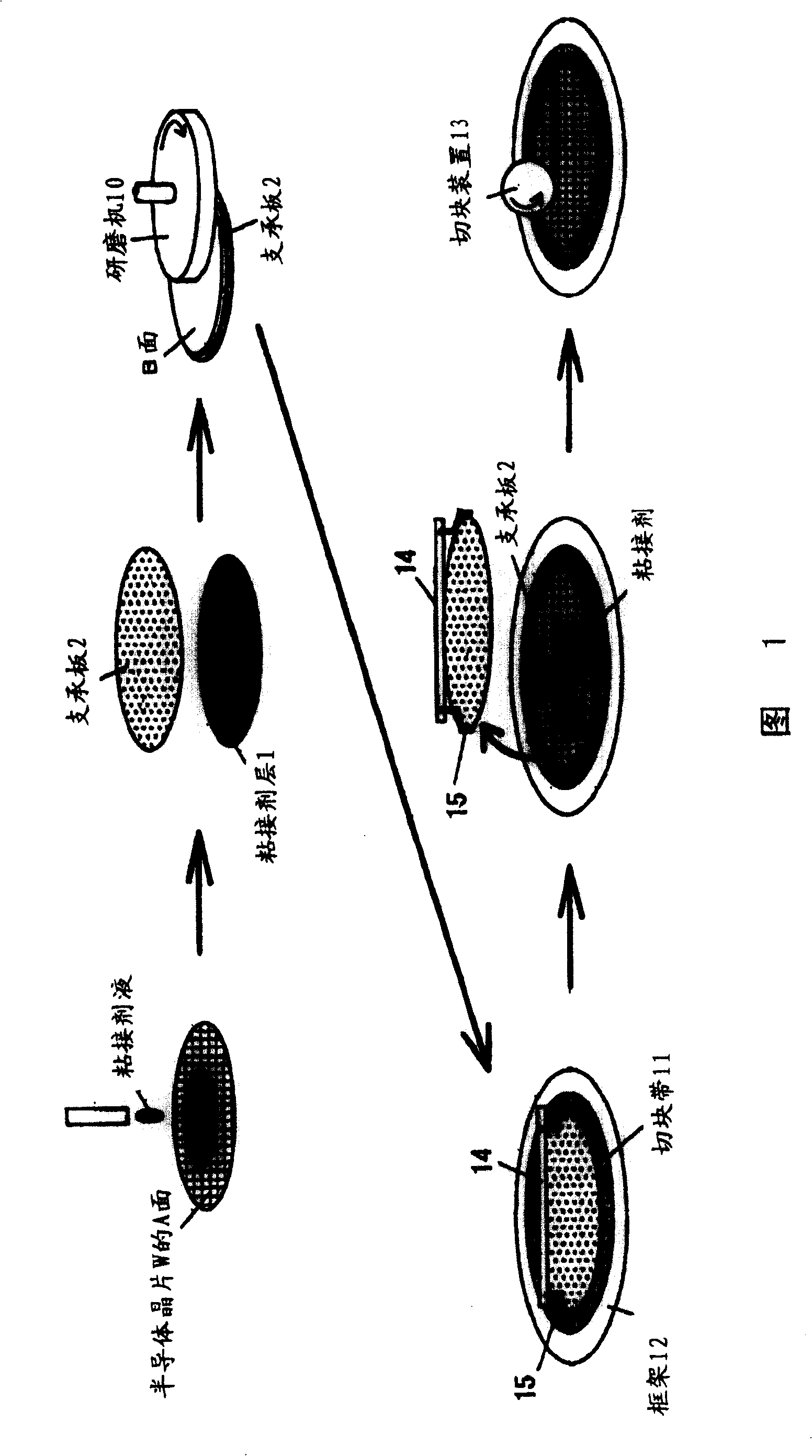
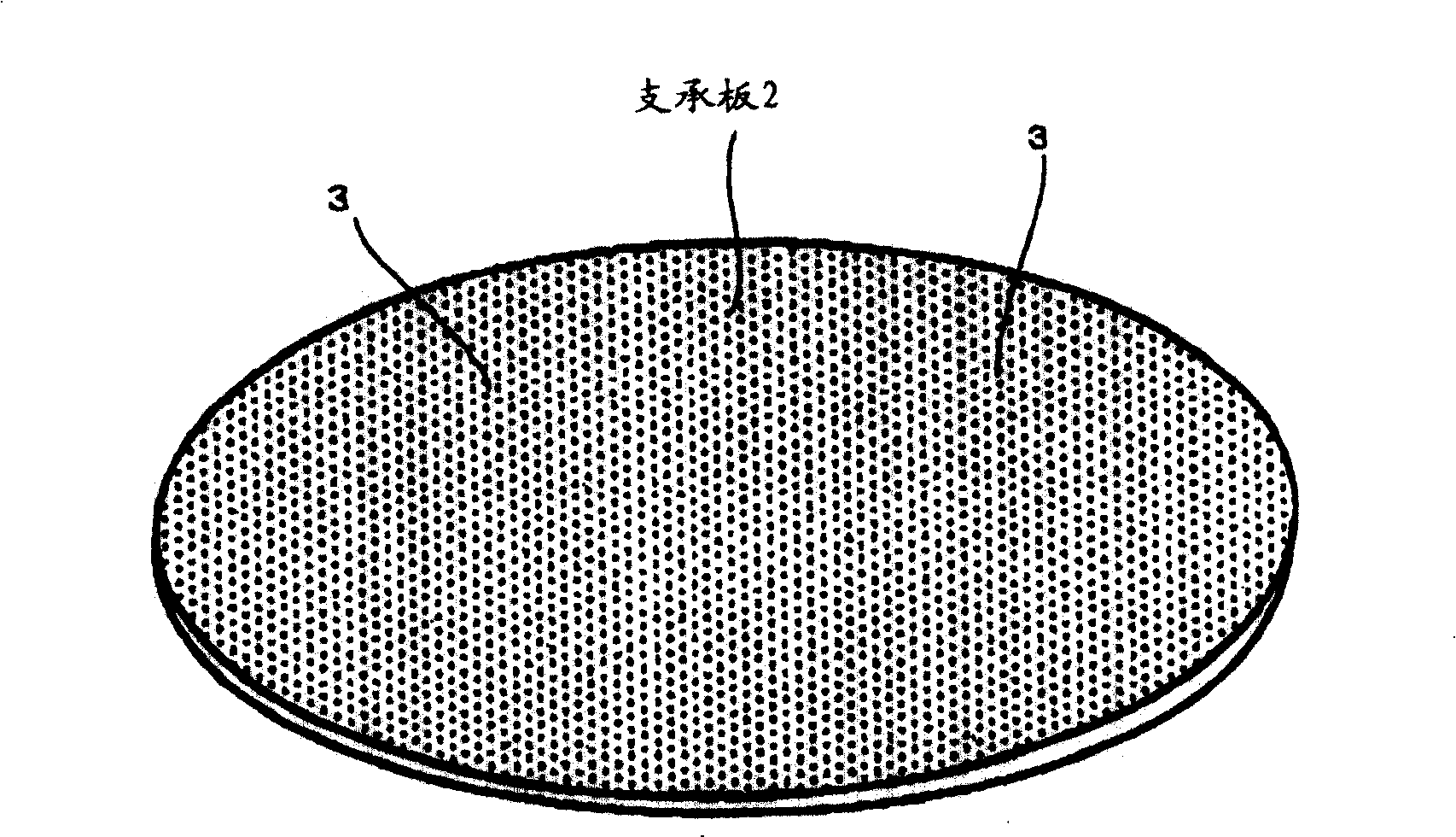
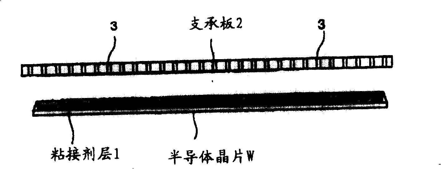
[0019] Embodiments of the present invention will be described below based on the drawings. FIG. 1 is a diagram illustrating a thinning process of a semiconductor wafer using a bonding apparatus of the present invention, figure 2 is a perspective view of the support plate, image 3 It is a side view showing the relationship between the substrate, the adhesive, and the support plate, and first, the overall thinning process will be described.

[0020] First, an adhesive liquid is applied to the circuit (element) formation surface (A surface) of the semiconductor wafer W. For coating, for example a spinner is used. Examples of the adhesive liquid include novolak-type phenolic resin-based materials, but are not limited thereto. In addition, the thickness of the adhesive is about several μm to 100 μm.

[0021] Next, if image 3 As shown, the above-mentioned adhesive is baked to cure it, and the adhesive layer 1 whose fluidity is eliminated is formed on the front surface of the ...


PUM

PropertyMeasurementUnit
thicknessaaaaaaaaaa

Abstract

To provide an adhering apparatus for pressure-bonding a support plate while easily removing the gas held between a substrate such as semiconductor wafer or the like and the support plate. A pressure reducing chamber 50 is connected with an evacuation apparatus via a pipe 51, allows formation of a carrying-in / out aperture 52 at its one side surface, and opens or closes this aperture 52 with a shutter 53. This shutter 53 is moved upward and downward with a cylinder unit 54 and when it is pushed with a pusher 55 from a side at the lifted position, a seal provided at the internal side surface of the shutter 53 is placed in close contact with the circumference of the aperture 52 to seal the inside of the chamber 50. When the pusher 55 is moved backward and the shutter 53 is moved downward, the aperture 52 is opened and a laminate of the wafer W and support plate 2 is carried in and out using a transferring apparatus under the above state. Within the chamber 50, a holding base 56 and a pressuring plate 57 are arranged for pressure-bonding the laminate.

Description

technical field [0001] The present invention relates to an apparatus for attaching a support plate to a substrate for support when thinning a substrate such as a semiconductor wafer. Background technique [0002] IC cards and mobile phones are required to be thinner, smaller, and lighter. In order to meet the requirements, semiconductor chips to be assembled must also be made thin. Therefore, at present, the thickness of a wafer serving as a base of a semiconductor chip is 125 μm to 150 μm, but it is said that the thickness for the next-generation chip must be 25 μm to 50 μm. [0003] In the step of thinning the semiconductor wafer with a grinder or the like, it is necessary to support the circuit formation surface side of the semiconductor wafer with a tape or a plate. Patent Document 1 discloses an apparatus for sticking a support plate on a semiconductor wafer. [0004] In the apparatus disclosed in Patent Document 1, a pair of upper and lower heating plates is arranged...

Claims


Application Information

Patent Timeline
Patent Type & Authority Patents(China)
IPC IPC(8): H01L21/00H01L21/02B32B37/00B30B12/00
CPCH01L21/67011H01L21/6835H01L2221/68327H01L2221/6834
Inventor 佐佐木保稻尾吉浩宫成淳
Owner 艾美柯技术株式会社
Why Eureka
Try Eureka