Chip testing mechanism and related method

A technology of chip testing and mechanism, applied in the direction of digital circuit testing, electronic circuit testing, measuring electricity, etc., can solve the problem of high manufacturing cost of electronic devices, expensive external high-frequency tester, high cost of high-frequency tester, etc. problems, to achieve the effect of saving manufacturing costs

Active Publication Date: 2009-02-11
VIA TECH INC
View PDF6 Cites 0 Cited by
  • Summary
  • Abstract
  • Description
  • Claims
  • Application Information

AI Technical Summary

Problems solved by technology

However, the external high-frequency tester is very expensive, so the production and manufacturing costs of electronic devices will remain high
For example, to test a chipset with a super-speed transmission bus, its tester needs to be able to handle high-frequency signals of 2GHz (because the super-speed transmission bus transmits data at 2GHz), and the cost of this high-frequency tester is very high

Method used


Image

  • Chip testing mechanism and related method
  • Chip testing mechanism and related method
  • Chip testing mechanism and related method

Examples


Embodiment Construction

[0017] Hereinafter, embodiments of the present invention will be described in detail with reference to the drawings.

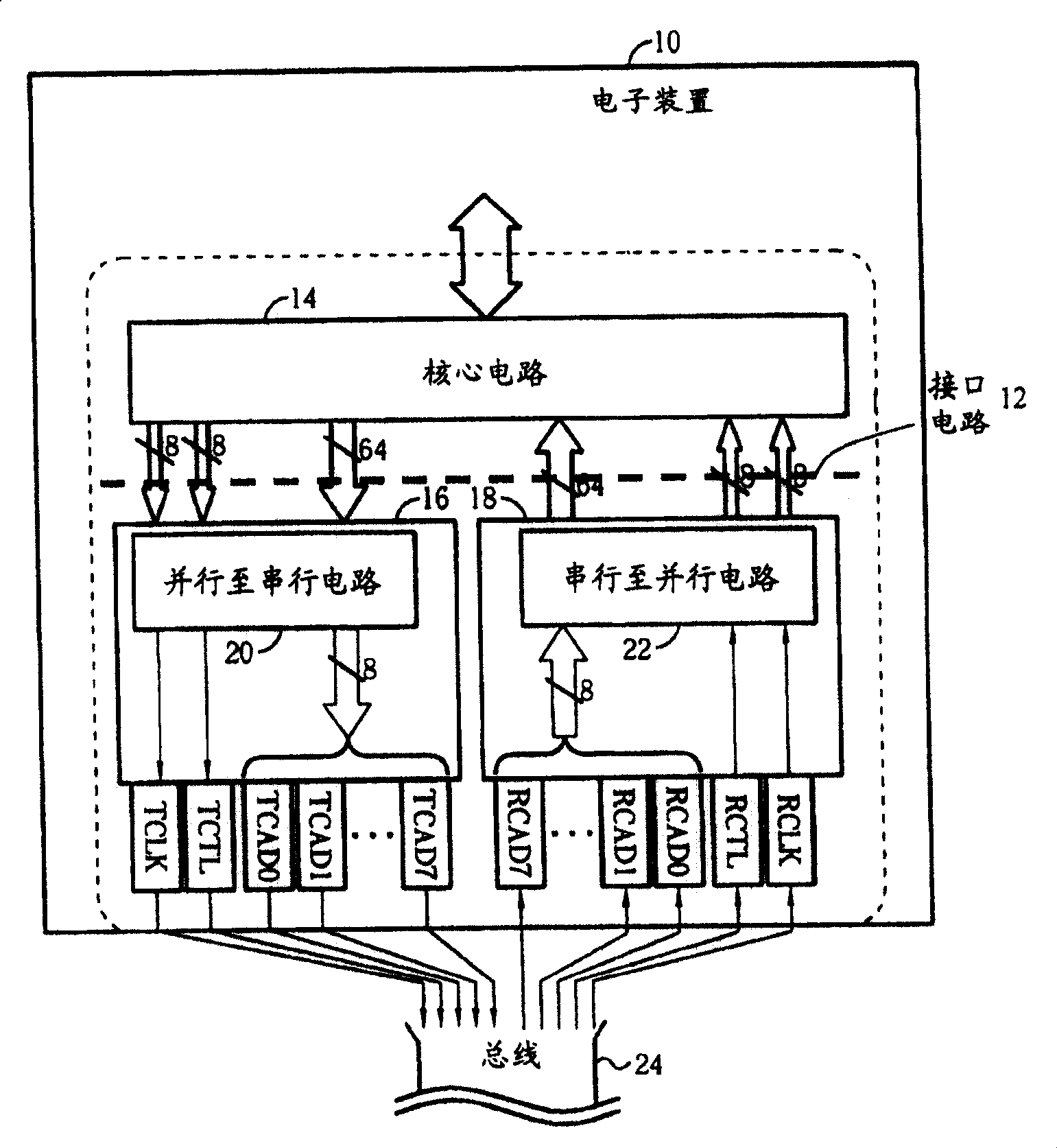
[0018] Please refer to figure 1 ; figure 1 is a schematic diagram of an electronic device 10 with a high-speed bus interface circuit. The electronic device 10 includes a high-speed bus interface circuit 12 and a core circuit 14 . The electronic device 10 may be a chip in an electronic system, such as a chipset in a computer system, and the high-speed bus interface circuit 12 enables the electronic device 10 to exchange information with other electronic devices (not shown) via the high-speed bus 24 with signal. The core circuit 14 is used to master encoding / decoding and control matters related to bus access (eg, determine whether to respond and when to respond after receiving an access request from the bus). In the present invention, the high-speed bus 24 can be a Hyper Transport Bus. In the high-speed bus interface circuit 12, a transmission circuit 16 an...


PUM


Abstract

The related chip testing method comprises: building inner loop in interface circuit of high-speed bus, sending information for I / O testing, and receiving the information by former inner loop to validate the chip I / O function and time sequence. This invention can save cost greatly and fit to take full-function I / O testing even in wafer stage.

Description

technical field [0001] The invention relates to a chip testing mechanism and a related method, in particular to a chip testing mechanism and a related method capable of being connected to a high-speed bus at low cost. Background technique [0002] In the electronic system, different electronic devices exchange information with each other through the bus, so that the electronic devices can coordinate operations and integrate their respective functions to complete the overall function of the electronic system. For example, in a computer system, the central processing unit is bridged to other peripheral devices (such as hard disk drives, optical drives, graphics accelerator cards, etc.) The interconnection with the bus enables the above-mentioned electronic devices to operate in an integrated manner. Of course, in the modern information society that emphasizes efficiency, the performance requirements for electronic systems are also increasing. In order to improve the overall ...

Claims


Application Information

Patent Timeline
Patent Type & Authority Patents(China)
IPC IPC(8): G01R31/28G01R31/317G01R31/3185G06F11/267
Inventor 苏俊源
Owner VIA TECH INC
Why Eureka
Try Eureka