Method for producing white light luminous diode

A technology of light emitting diodes and a manufacturing method, which is applied to electrical components, circuits, semiconductor devices, etc., can solve problems such as inability to use, inconvenience, and edge defects of the fluorescent layer 23, and achieve the effect of increasing the value of the manufacturing method and making it widely available.

Active Publication Date: 2009-03-25
BRIGHT LED ELECTRONICS CORP +1
View PDF9 Cites 0 Cited by
  • Summary
  • Abstract
  • Description
  • Claims
  • Application Information

AI Technical Summary

Problems solved by technology

[0009] However, the above method can only be applied to flip chips that do not need to be connected by gold wires, and cannot be used on chips that are generally connected by gold wires.
[0010] Moreover, in actual production, when the template 24 is separated from the substrate 21, the edge of the opening 241 will pull the phosphor layer 23 and cause defects on the edge of the phosphor layer 23, so as to affect the uniformity of the white light emitted by the light emitting diode.
[0011] It can be seen that the above-mentioned existing white light emitting diode manufacturing method obviously still has inconvenience and defects in method and use, and needs to be further improved urgently.
In order to solve the above-mentioned problems, the relevant manufacturers have tried their best to find a solution, but no suitable design has been developed for a long time, and the general method has no suitable production method to solve the above-mentioned problems. This is obviously a problem. Issues that relevant industry players are eager to solve

Method used


Image

  • Method for producing white light luminous diode
  • Method for producing white light luminous diode
  • Method for producing white light luminous diode

Examples


Embodiment Construction

[0045] In order to further explain the technical means and effects of the present invention to achieve the intended purpose of the invention, the specific implementation methods, methods, steps, Features and their functions are described in detail below.

[0046] see Figure 4 and Figure 5 As shown, the manufacturing method of the white light emitting diode of the preferred embodiment of the present invention mainly includes the following steps:

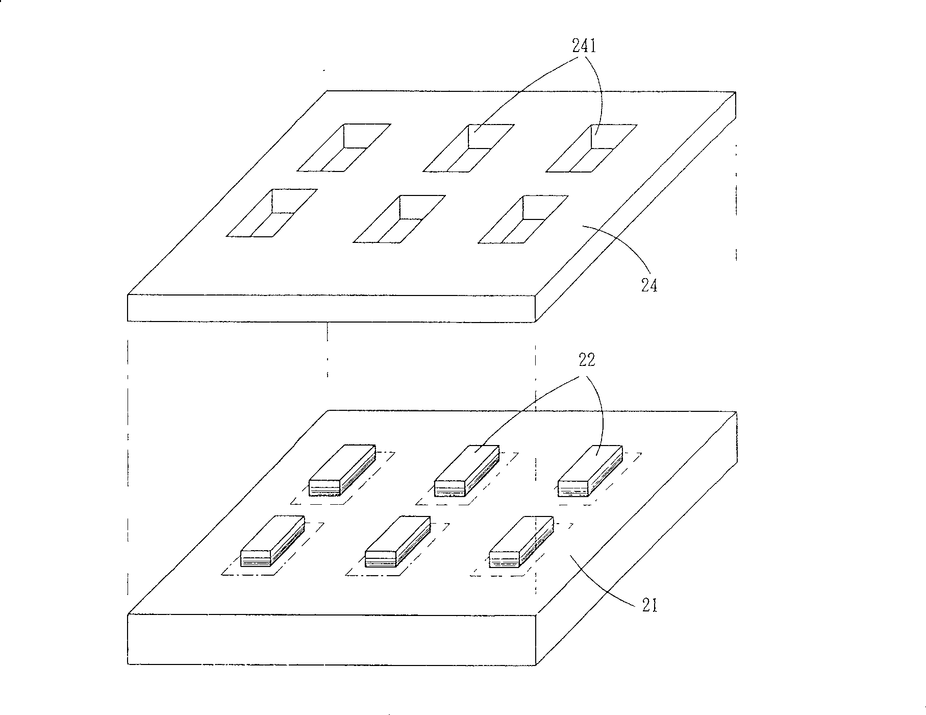
[0047] First, step 41 first provides the base 31;

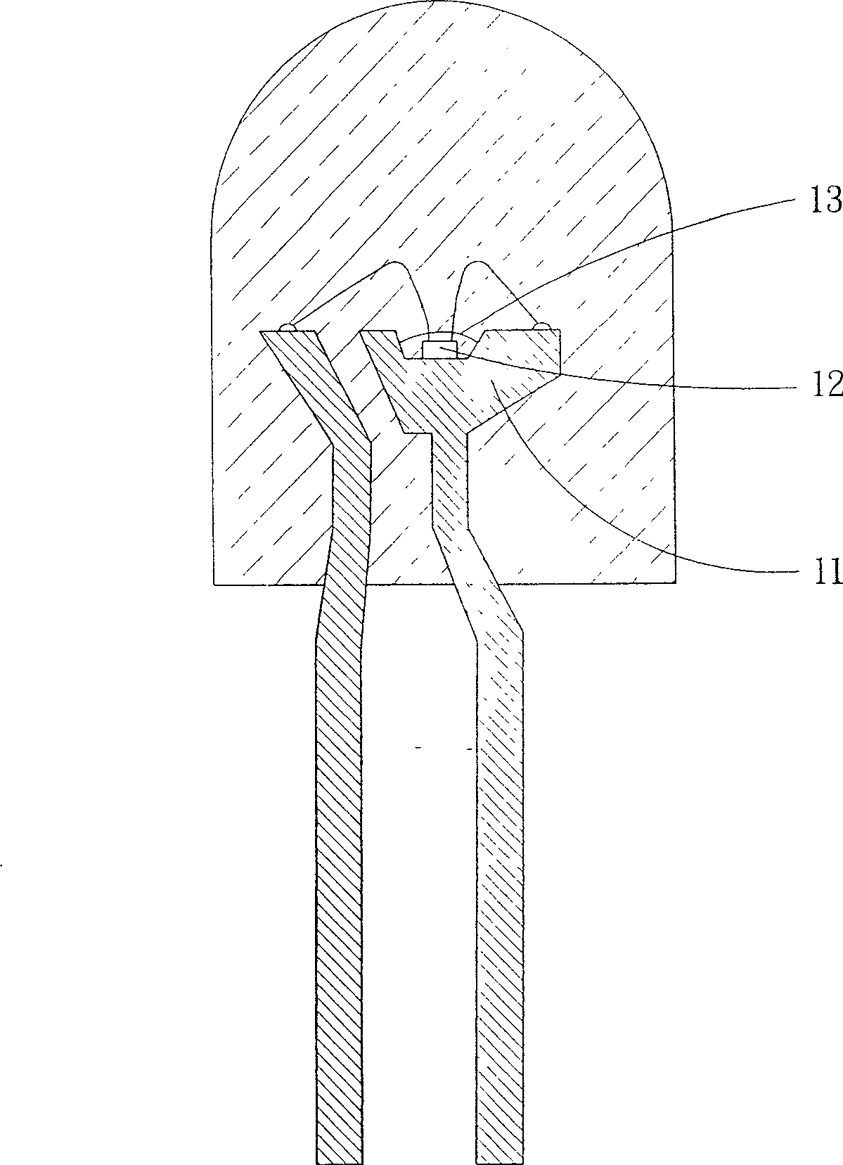
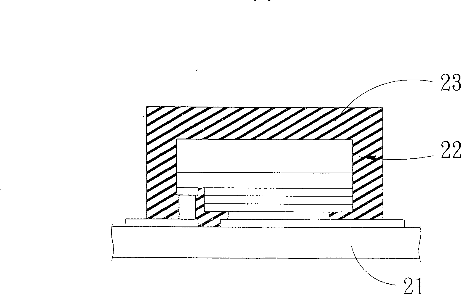
[0048] Then, in step 42 , the LED die (hereinafter referred to as die) 32 is bonded on the base 31 . The way of bonding is to first place the silver glue as an adhesive material on the base 31, then set the crystal grains 32 on the silver glue, and finally make the silver glue heat and solidify. The conventional eutectic alloy (Eutectic) bonding can also be used for the above-mentioned grain bonding method.

[0049] Next, see Figure 4 , Image 6 and Figure 7 As shown, ste...


PUM


Abstract

The invention relates to a preparing method of white light LBD that includes following steps: (A) providing a basis; (B) a LBD grain is set on said basis; (C) an outer fluorescence wall is set on said basis and surrounds said LBD grain; and (D) a inner fluorescence layer is set in space which is defined by said outer fluorescence wall, and fills said space. The invention divides the production of fluorescence layer into two steps, firstly setting an outer fluorescence wall at around of LBD grain, then forming an inner fluorescence layer in space defined by the outer fluorescence wall to compose an integral fluorescence layer whose thickness is even, defining figuration of the integral fluorescence layer by setting the outer fluorescence wall to control the thickness of the integral fluorescence layer possess consistency, the white light LBD can emit even white light, it resolves problem that white light emitted by ago LBD is not even.

Description

technical field [0001] The invention relates to a method for manufacturing a white light emitting diode, in particular to a method for manufacturing a fluorescent layer of a light emitting diode capable of emitting uniform white light. Background technique [0002] Light-emitting diodes (ie, diodes) have the advantages of small size, light weight, good shock resistance, and fast response, and can be widely used as light sources for various indicators and displays. In particular, the white light emitting diodes developed in recent years tend to replace general tungsten bulbs or fluorescent tubes as lighting sources. [0003] U.S. Patent No. 5,998,925 proposes a technical solution, which is a white light-emitting diode that uses a blue light-emitting diode grain with a phosphor layer. The phosphor layer can absorb part of the blue light emitted by the light-emitting diode grain and convert it It is yellow light, so that the yellow light converted by the fluorescent layer can ...

Claims


Application Information

Patent Timeline
Patent Type & Authority Patents(China)
IPC IPC(8): H01L33/00H01L33/30H01L33/48
Inventor 张铭利廖宗仁陈炎成曾庆霖
Owner BRIGHT LED ELECTRONICS CORP
Why Eureka
Try Eureka