Manufacturing method of wafer level testing circuit board and structure thereof

A technology for testing circuit boards and manufacturing methods, which is applied in the direction of measuring electricity, measuring electrical variables, and electronic circuit testing, etc. question

Active Publication Date: 2009-07-01
VISERA TECH CO LTD
View PDF3 Cites 0 Cited by
  • Summary
  • Abstract
  • Description
  • Claims
  • Application Information

AI Technical Summary

Problems solved by technology

[0003] Commonly used tests for CSP components can only be conducted one by one for a single component, or the test equipment supplier provides a special test board and test machine for multiple CSP components to be placed, and then completes the correct electrical test on the hardware. Only by cooperating with the special hardware control production process program and test software of the equipment supplier, can a single fast electrical test be carried out on multiple CSP components. Such additional electrical test equipment will not only cost costs, but also component manufacturing. The factory itself cannot accurately control the electrical specifications of the electrical measurement equipment. The actual electrical measurement results of the CSP components are often changed due to the electrical drift of any electronic part on the electrical measurement equipment. Even if any hardware part in the equipment machine Faults can also easily affect the electrical test results and be judged as defective CSP components for a while, reducing the production quality. In severe cases, it will even lead to reimbursement losses for mass-produced components. Therefore, component manufacturers have high-precision electronic components that are self-manufactured. It is really difficult to achieve effective full-process control on the electrical measurement program

Method used


Image

  • Manufacturing method of wafer level testing circuit board and structure thereof
  • Manufacturing method of wafer level testing circuit board and structure thereof
  • Manufacturing method of wafer level testing circuit board and structure thereof

Examples


Embodiment Construction

[0021] Hereinafter, a preferred embodiment is enumerated in conjunction with some accompanying drawings, in order to further illustrate the components and effects of the present invention as follows:

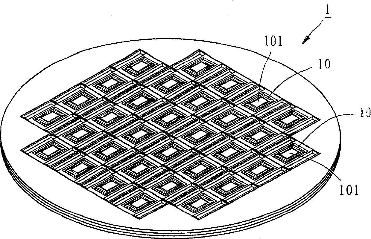
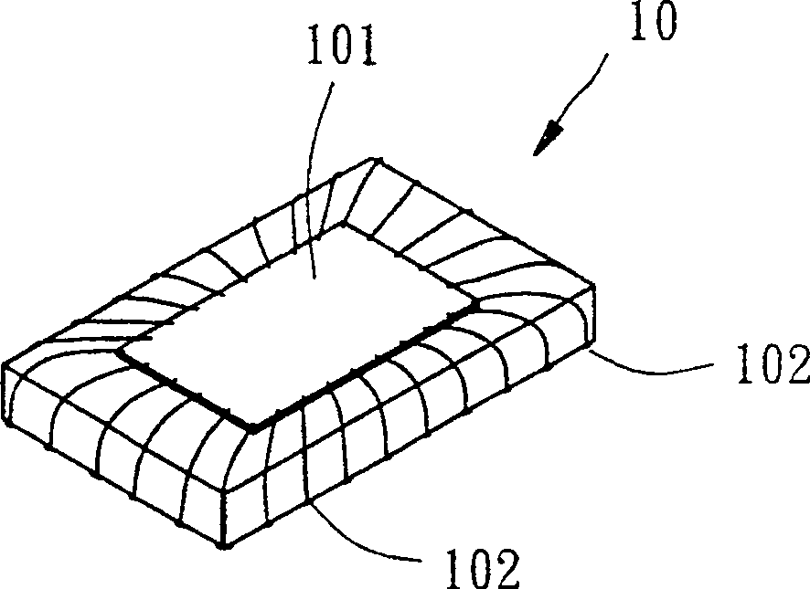
[0022] see Figure 1 to Figure 7 Shown is a test circuit board 1 of the first preferred embodiment provided by the present invention, which can perform wafer-level testing on a plurality of electronic components 10 packaged in modules. These electronic components 10 exemplified in this embodiment are fabricated The integrated circuit chip of each image sensor chip 101 is a modular package assembly after the chip size package (Chip Size Package, CSP) manufacturing process, refer to figure 2 , and there are a plurality of conductive bumps 102 on it, as a connection medium for each image sensor chip 101 to be electrically connected to the external circuit; the following is a further description of the manufacturing steps of the test circuit board 1:

[0023] a. Please see if im...


PUM


Abstract

A manufacturing method of a wafer-level test circuit board of the present invention is to define a plurality of accommodating areas similar to the distribution of integrated circuit chips in a wafer on a printed circuit board, and extend and arrange a plurality of wires on each accommodating area to the corresponding peripheral area. On the detection area, set at least one test soldering point corresponding to the detection area on each wire, and set at least one bump soldering point corresponding to the accommodation area, and set each electronic component after the chip size packaging manufacturing process on the accommodation area , so that the conductive bumps of each electronic component are electrically connected to the bump solder joints, that is, the probes of the probe card can contact each test solder joint, and the electrical test of each electronic component can be quickly completed like a wafer-level test method.

Description

technical field [0001] The invention relates to an electronic circuit testing system, in particular to a circuit board structure for wafer-level testing of electronic components after a chip size packaging manufacturing process. Background technique [0002] Component testing in general integrated circuit chip manufacturing plants can be divided into front-end wafer testing in the manufacturing process stage and back-end packaging testing after chip module packaging. Among them, under the long-term development and improvement of wafer testing, the wafer-level testing system used has been developed. It can achieve high-efficiency and high-precision electrical measurement quality, so it has excellent benefits for the production capacity control of the entire wafer manufacturing process stage; in terms of packaging and testing, there are wafer-level packaging (Wafer Level Package, WLP) manufacturing process and The electrical test after the chip size package (Chip Size Package,...

Claims


Application Information

Patent Timeline
Patent Type & Authority Patents(China)
IPC IPC(8): G01R1/073G01R1/067G01R31/00G01R31/28G01R31/26H01L21/66
Inventor 卢笙丰萧玉焜
Owner VISERA TECH CO LTD
Why Eureka
Try Eureka