Method for preventing etching or corrosion of metallic titanium in screen layer

A technology of metal titanium and barrier layer, which is applied in the field of semiconductor integrated circuit technology, can solve problems such as reduction of contact surface, influence on yield rate, reliability problems, etc., and achieve the effect of preventing etching and improving adhesion performance

Inactive Publication Date: 2009-08-05
SHANGHAI HUAHONG GRACE SEMICON MFG CORP
View PDF4 Cites 0 Cited by
  • Summary
  • Abstract
  • Description
  • Claims
  • Application Information

AI Technical Summary

Problems solved by technology

[0013] 1) The contact surface between the through hole and the upper metal is reduced, the contact resistance is increased, and the yield rate is affected
[0014] 2) Due to the reduction of the contact surface between the through hole and the upper metal, the current density of the contact point is higher than normal during the use of the product, which may shorten the life of the product and cause reliability problems

Method used


Image

  • Method for preventing etching or corrosion of metallic titanium in screen layer
  • Method for preventing etching or corrosion of metallic titanium in screen layer
  • Method for preventing etching or corrosion of metallic titanium in screen layer

Examples


Embodiment Construction

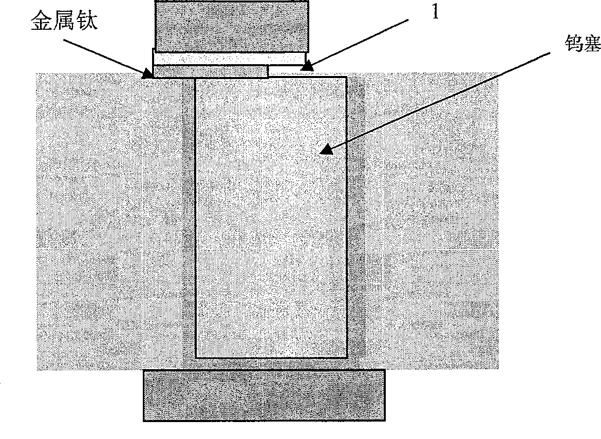
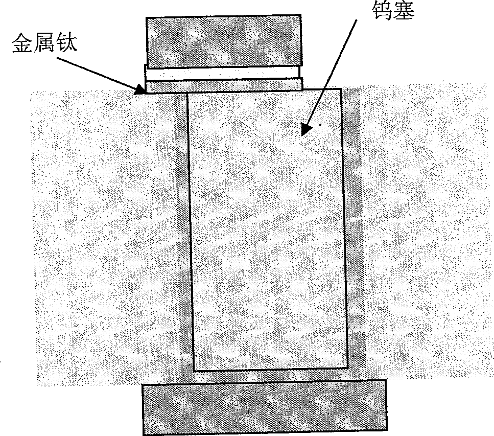
[0023] The study found that the plasma radio frequency (RF) treatment process before sputtering of titanium in the barrier layer has a significant impact on the surface roughness of the tungsten plug, thus affecting the adhesion between titanium and tungsten plug. If the method of optimizing the RF treatment process can effectively improve the adhesion performance of titanium and tungsten plugs, and then achieve the purpose of preventing etching. Just based on the above design, the method of the present invention proposes to optimize the RF processing technology.

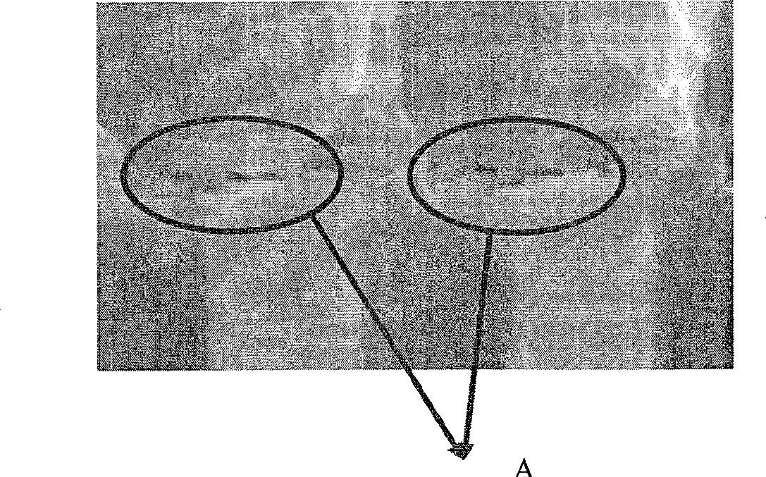
[0024] First, the RF treatment process before TI sputtering can be removed. At this time, it is available from the attached image 3 It can be seen that the titanium metal is intact at this time.

[0025] Secondly, in the RF treatment before TI's sputtering, the process conditions in the RF treatment can be controlled in the following range: SiO 2 The loss is 0-60 angstroms, the temperature is 260°C-320°C, the fl...


PUM


Abstract

The invention discloses a method for preventing metal titanium in a barrier layer from being etched or corroded, which can improve the adhesion performance between TI and tungsten plugs, thereby achieving the purpose of preventing TI from being etched or corroded. The method is mainly to optimize the plasma radio frequency treatment process of metal titanium in the barrier layer before sputtering. The optimization is to remove the plasma RF treatment process. The optimization is to control the plasma radio frequency treatment process conditions in the following ranges: SiO2 loss is 0-60 angstroms, temperature is 260C-320C, flow of Ar is 25-40sccm, power supply is 100-220W.

Description

technical field [0001] The invention relates to the technical field of semiconductor integrated circuit technology, in particular to a method for preventing metal titanium (Ti) in a barrier layer (BARRIER layer) from being etched or corroded. Background technique [0002] In the current semiconductor process, there is such a process to realize metal-metal interconnection, and the process is: [0003] 1) After the lower metal wiring pattern is formed, the deposition and planarization of the interlayer film are completed. [0004] 2) Holes are formed by photolithography and etching of vias after planarization. [0005] 3) After the via hole is formed, a tungsten plug is formed by depositing a barrier film for the via hole and tungsten and chemical-mechanical polishing of the tungsten. [0006] 4) After the tungsten plug is formed, a metal barrier layer (composed of titanium and titanium nitride) and a metal layer (composed of aluminum) are formed by a sputtering process, and...

Claims


Application Information

Patent Timeline
Patent Type & Authority Patents(China)
IPC IPC(8): C23C14/02
Inventor 肖胜安徐继寅何奕华吕煜坤
Owner SHANGHAI HUAHONG GRACE SEMICON MFG CORP
Why Eureka
Try Eureka