
Semiconductor device and method of manufacturing the same

A semiconductor and electrode technology, which is applied in semiconductor/solid-state device manufacturing, semiconductor devices, semiconductor/solid-state device components, etc., can solve problems such as inability to achieve conduction, and achieve the effect of preventing etching

Inactive Publication Date: 2008-07-16
ROHM CO LTD
View PDF1 Cites 2 Cited by
  • Summary
  • Abstract
  • Description
  • Claims
  • Application Information

AI Technical Summary

Problems solved by technology

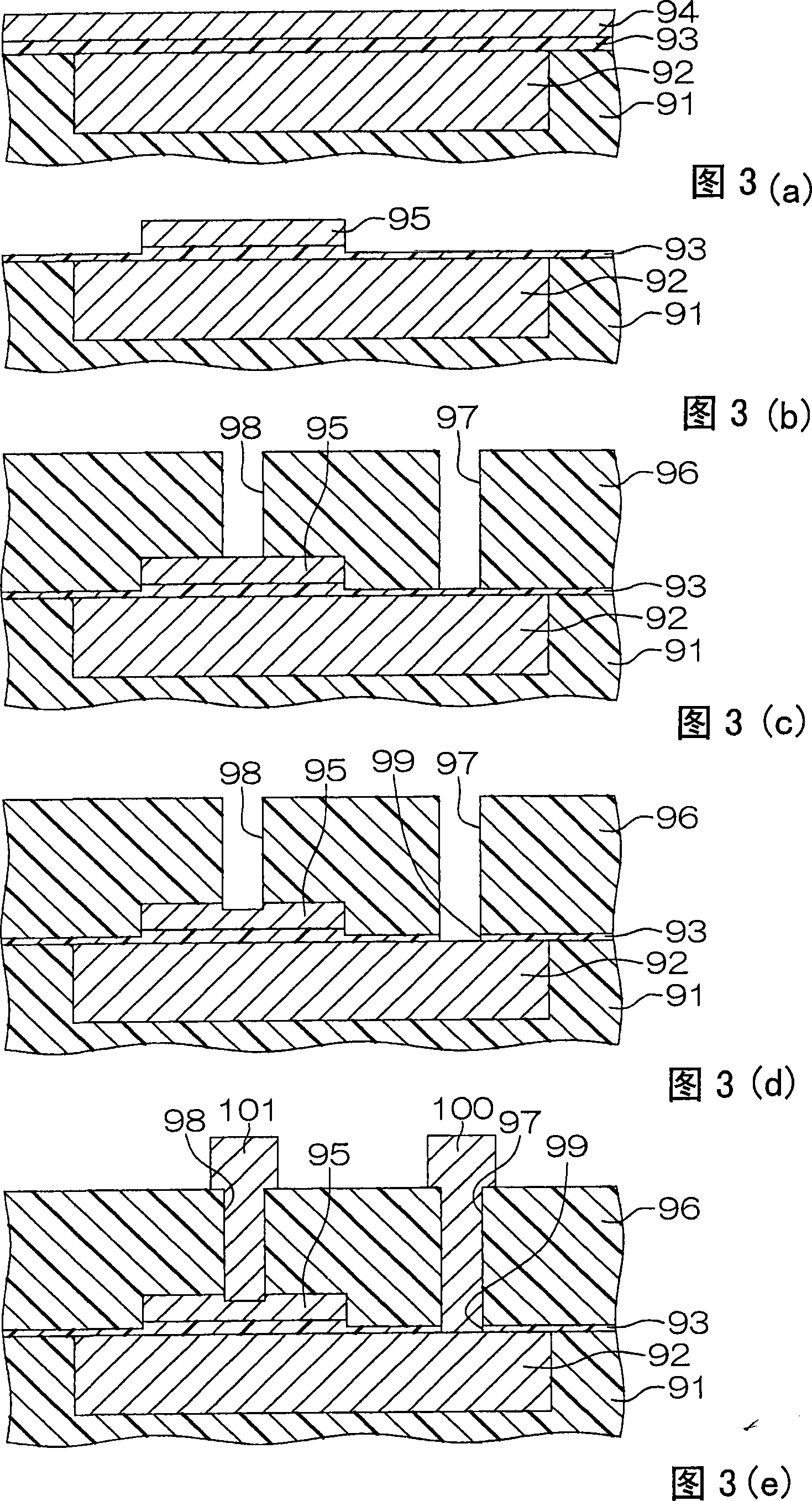
Conversely, if the etching time is set shorter, the opening 99 cannot be formed in the capacitive film 93, and there is a possibility that the conduction between the lower electrode 92 and the lower electrode contact plug 100 cannot be realized.

Method used


Image

  • Semiconductor device and method of manufacturing the same
  • Semiconductor device and method of manufacturing the same
  • Semiconductor device and method of manufacturing the same

Examples


Embodiment Construction

[0041] Hereinafter, embodiments of the present invention will be described in detail with reference to the drawings.

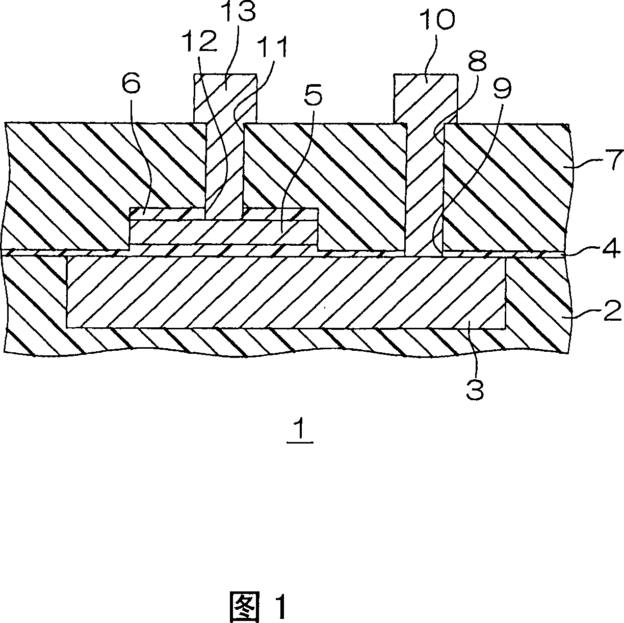
[0042] FIG. 1 is a cross-sectional view schematically showing the structure of a semiconductor device according to an embodiment of the present invention.

[0043] In this semiconductor device 1, a semiconductor substrate (not shown) mounted with a functional element such as a MOSFET (Metal Oxide Semiconductor Field Effect Transistor) made of SiO 2 (silicon oxide) interlayer insulating film 2. As the material of the interlayer insulating film 2 , for example, a Low-k film material such as SiOC (carbon-doped silicon oxide) or SiOF (fluorine-doped silicon oxide) may be used.

[0044] A lower electrode 3 made of Cu is embedded in the surface layer portion of the interlayer insulating film 2 . The surface of the lower electrode 3 is substantially flush with the surface of the interlayer insulating film 2 .

[0045] A capacitive film 4 made of SiN is laminated o...


PUM


Abstract

The semiconductor device according to the present invention includes a lower electrode made of a metallic material, a capacitance film made of an insulating material and laminated on the lower electrode, an upper electrode made of a metallic material, opposed to the lower electrode through the capacitance film, and having an outline smaller than that of the lower electrode in plan view along the opposed direction, and a protective film made of the same material as that of the capacitance film and laminated on the upper electrode.

Description

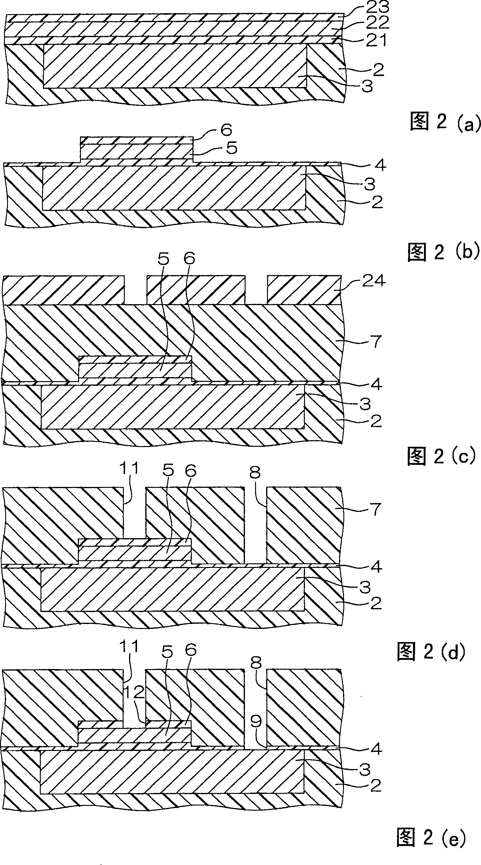
technical field [0001] The present invention relates to a semiconductor device having a capacitor element having a MIM (Metal-Insulator-Metal) structure and a method for manufacturing the same. Background technique [0002] A capacitive element with an insulating capacitive film sandwiched between the lower electrode and the upper electrode (MIM structure) has a small resistance component and can achieve high capacitance density, so it is attracting attention as a capacitive element mounted in a wireless communication system LSI. [0003] As a capacitive element with an MIM structure, the lower electrode and the upper electrode are generally formed of a metal film including Al (aluminum), but in order to further reduce the resistance, the material of the lower electrode has been studied, and Cu (copper) with higher conductivity is used. instead of Al. [0004] 3( a ) to 3 ( e ) are schematic cross-sectional views showing, in order of steps, the manufacturing steps of a semi...

Claims


Application Information

Patent Timeline
IPC IPC(8): H01L29/92H01L23/522H01L27/04H01L27/06H01L27/08H01L21/02H01L21/768H01L21/822
CPCH01L2924/0002H01L28/40H01L2924/00
Inventor 八木良太郎中尾雄一西村勇
Owner ROHM CO LTD
Learn More