Method for processing precision patterns

A pattern and precise technology, applied in the field of manufacturing process, can solve problems such as unreachable, and achieve the effect of simplifying the degree of difficulty

Inactive Publication Date: 2013-06-05
华映视讯(吴江)有限公司 +1
View PDF7 Cites 0 Cited by
  • Summary
  • Abstract
  • Description
  • Claims
  • Application Information

AI Technical Summary

Problems solved by technology

However, the precision of exposure machines currently used in the panel industry is usually 3 μm. Taking the positive photoresist as an example, the line spacing S of the upper transparent conductive layer 140 can only reach 3 μm, which is the current limit
In other words, it is impossible to make the upper transparent conductive layer 140 with the line width W and the line spacing S less than 3 μm.

Method used


Image

  • Method for processing precision patterns
  • Method for processing precision patterns
  • Method for processing precision patterns

Examples


Embodiment Construction

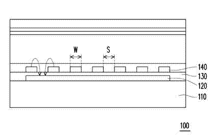
[0022] Generally speaking, when the lithographic etching process is carried out through the exposure machine, it may be limited by the design of the machine itself or the optical limitation of the exposure conditions, so the line width and spacing of the formed pattern will be limited. In this way, if it is desired to design a pattern with higher fineness, it will be difficult, such as the structure and content described in the prior art. Based on this, an embodiment of the present invention proposes a process method, which can still produce patterns with finer line width and spacing under the exposure conditions of the original exposure machine. The description is as follows, wherein this embodiment is based on A plurality of transparent conductive patterns are formed as an example.

[0023] Figures 2A-7A It is a top view of a process flow of a manufacturing method according to an embodiment of the present invention, which is suitable for making a precise pattern, and Fig...


PUM


Abstract

The invention provides a method for processing precision patterns. The method at least comprises the following steps: firstly, forming a first crystallizable material layer on a substrate; secondly, patterning the first crystallizable material layer so as to form a plurality of first patterns on the substrate, wherein the space between any two adjacent first patterns is more than the width of each first pattern; thirdly, carrying out first processing on the first patterns to crystallize the first patterns; fourthly, forming a second crystallizable material layer on the substrate, wherein the second crystallizable material layer covers the first patterns; and fifthly, patterning the second crystallizable material layer so as to form a plurality of second patterns on the substrate, wherein each second pattern is arranged between the first patterns.

Description

technical field [0001] The present invention relates to a process method, and in particular to a precision pattern process method. Background technique [0002] figure 1 It is a partial cross-sectional view of a liquid crystal display panel. Please refer to figure 1 The liquid crystal display panel 100 is, for example, a Fringe Field Switching (FFS) liquid crystal display panel, which at least includes a substrate 110 , a lower transparent conductive layer 120 , an insulating layer 130 and an upper transparent conductive layer 140 . The lower transparent conductive layer 120 is disposed on the substrate, the insulating layer 130 covers the lower transparent conductive layer 120 , and the upper transparent conductive layer 140 is disposed on the insulating layer 130 . [0003] exist figure 1 Among them, the line width of the upper transparent conductive layer 140 is W, and the line spacing is S. Generally speaking, finer line width W and line spacing S can obtain higher t...

Claims


Application Information

Patent Timeline
Patent Type & Authority Patents(China)
IPC IPC(8): H01L21/77H01L21/02
Inventor 张锡明
Owner 华映视讯(吴江)有限公司
Why Eureka
Try Eureka