

Chip packaging structure and method of producing the same
A technology of chip packaging structure and manufacturing method, applied in semiconductor/solid-state device manufacturing, electrical components, electrical solid-state devices, etc., can solve the problems of adhesive overflow contaminating solder pads and contaminating circuits, etc.
- Summary
- Abstract
- Description
- Claims
- Application Information
AI Technical Summary
Problems solved by technology
Method used
Image

Examples
Embodiment Construction
[0034] The detailed description is as follows, and the preferred embodiment is only for illustration and not intended to limit the present invention.
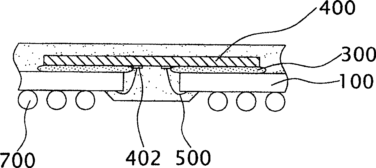
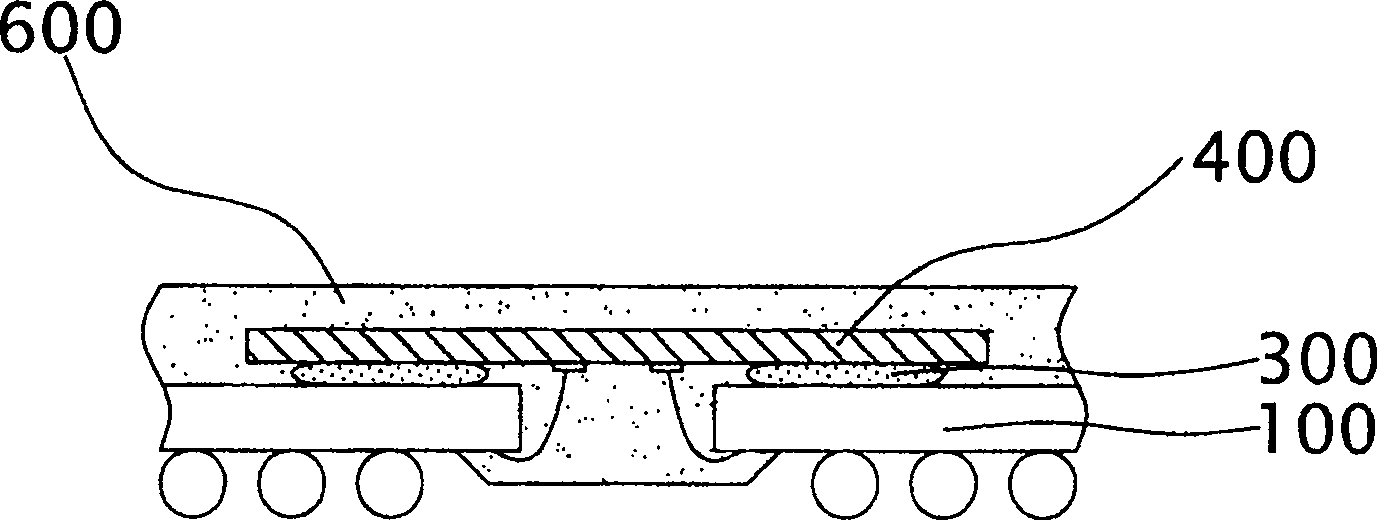
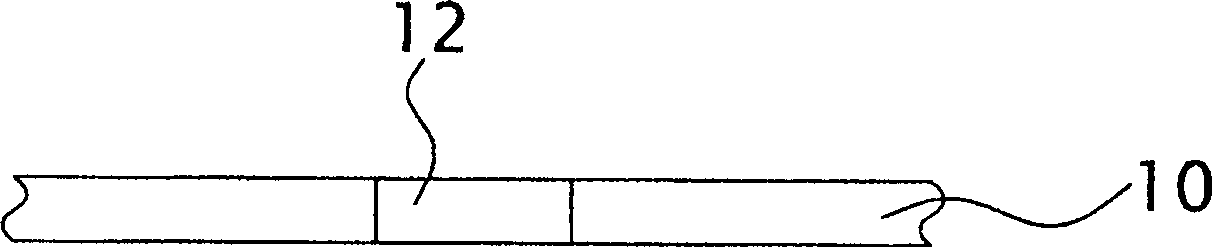
[0035] Figure 2A , Figure 2B , Figure 2C , Figure 2D , Figure 2E , Figure 2F , Figure 2G-1 and Figure 2G-2 Structural cross-sectional view of each step of the manufacturing method of the chip packaging structure according to an embodiment of the present invention. First, please refer to Figure 2A , provide a substrate 10, which is made of metal, glass, ceramics or polymer material, and has at least one opening 12 through the substrate 10, wherein the substrate 10 can be formed by using a suitable method to penetrate the substrate 10, or it can have at least one The commercialized structure of the opening 12.
[0036] Next, refer to Figure 2B , forming a blocking element 20 on the periphery of the opening 12 on the upper surface 11 of the substrate 10 . In one embodiment, the stop member 20 is formed by one of...
PUM
 Abstract
Description
Claims
Application Information