Radio-frequency switch

A switching, radio frequency signal technology, applied in the direction of electronic switches, electrical components, electrical solid devices, etc.

Inactive Publication Date: 2009-11-25
SUMITOMO ELECTRIC DEVICE INNOVATIONS
View PDF8 Cites 0 Cited by
  • Summary
  • Abstract
  • Description
  • Claims
  • Application Information

AI Technical Summary

Problems solved by technology

Therefore, it is no longer possible to use the conventional techniques disclosed in Documents 1 to 3, which have various breakdown voltage problems, to solve the above-mentioned problems.

Method used


Image

  • Radio-frequency switch
  • Radio-frequency switch
  • Radio-frequency switch

Examples


no. 1 example

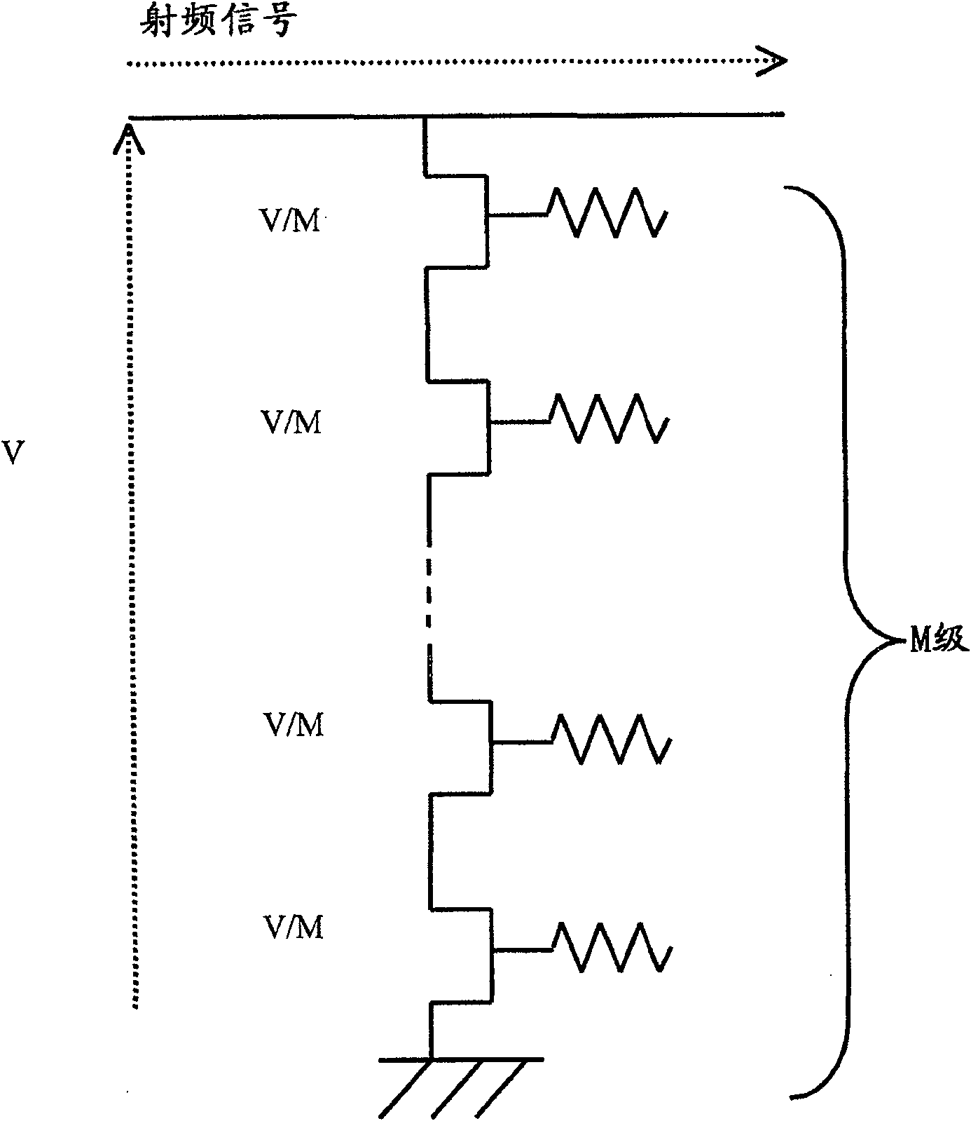
[0028] Figure 7A is a plan view of the radio frequency switch according to the first embodiment of the present invention. Figure 7A The RF switch in includes 3 stages of field effect transistors connected in series. Figure 7B represents a conventional RF switch with 3 stages of field effect transistors connected in series. As will be explained below, the electrode interconnection (interconnection) of the source or drain of a field effect transistor connected to an intermediate (second) stage is narrower than that connected to an initial (first) stage The source or drain of the field effect transistor and the width of the other electrode interconnection of a radio frequency line, or is connected to the source or drain of a field effect transistor of the last (third) stage and a ground line The width of the other electrode interconnection. The electrode interconnection connected to the source of the field effect transistor is called source. The electrode interconnection c...

no. 2 example

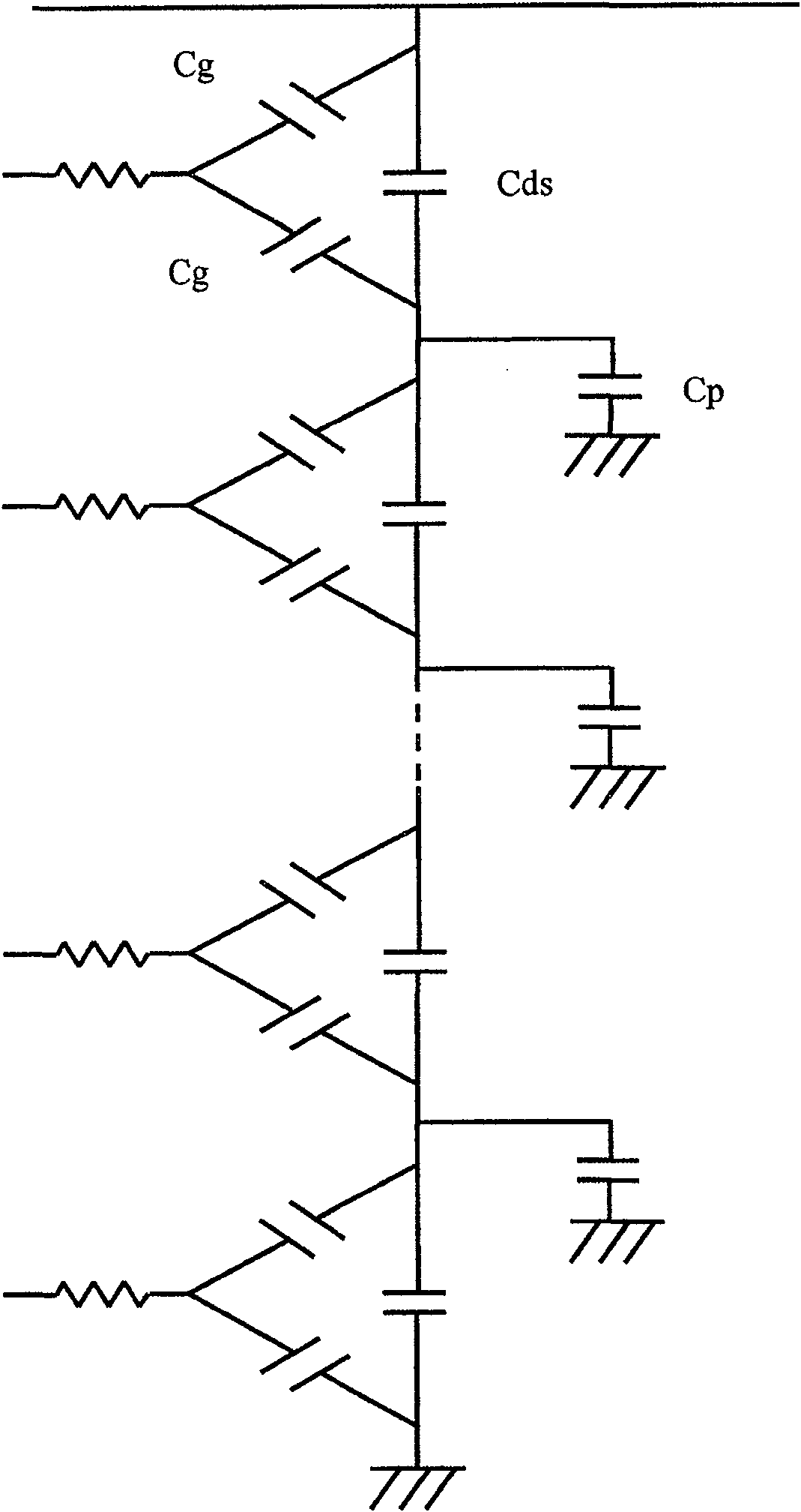
[0039] Figure 9 is a plan view of a radio frequency switch according to a second embodiment of the present invention. Hereinafter, in the second embodiment, the same components and configurations as those of the first embodiment have the same reference numerals. According to the second embodiment of the present invention, the field effect transistor formation region 16 provided at the intermediate stage (in this embodiment, the second stage) 2 The total gate width of the field effect transistors therein is set to be smaller than the total gate widths of the field effect transistors at the initial stage and the final stage. More specifically, the field effect transistor forming region 16 1 and 16 3 Each of these includes seven field effect transistors. In contrast, the field effect transistor forming region 16 2 Includes 6 field effect transistors. Therefore, with Figure 7A Compared to the circuit shown, it is possible to reduce the S / D electrode interconnection by 30 ...


PUM


Abstract

A switch for selectively changing a radio frequency signal includes at least three field effect transistors connected in series. The width of the source or drain provided at the intermediate stage is narrower than that of the source or drain provided at the starting stage and the last stage. Therefore, it is possible to reduce the parasitic capacitance to ground at the intermediate stage, and thereby it is possible to realize a switch with high processing power.

Description

technical field [0001] The present invention relates generally to radio frequency (RF) switches for radio frequency devices, such as mobile communication devices, and more particularly, to radio frequency switches having a plurality of field effect transistors (RF) connected in series thereon. Background technique [0002] In recent years, a radio frequency switch (SPNT: single pole N through: N indicates the number of ports) having a plurality of ports has been used in a mobile phone unit which communicates via a plurality of carrier frequency signals. RF switches include field effect transistors (FETs) made of various compound semiconductors. The RF switch is required to have low harmonic performance, more specifically -70dBc or below of the fundamental of the transmitted signal. In order to suppress the harmonic components to a low level, field effect transistors are required to improve the linearity of the resistance in the on-state and have excellent off-state power. ...

Claims


Application Information

Patent Timeline
Patent Type & Authority Patents(China)
IPC IPC(8): H03K17/687H01L27/04
Inventor 宫泽直行
Owner SUMITOMO ELECTRIC DEVICE INNOVATIONS
Why Eureka
Try Eureka