
Method for implementing chip test

A technology for chip testing and chips to be tested, applied in electronic circuit testing, electrical measuring, measuring devices, etc., can solve the problems of inflexible testing and high testing costs, and achieve the effects of flexible testing, streamlining workload, and simplifying complexity.

Inactive Publication Date: 2010-01-06
VIMICRO CORP
View PDF8 Cites 2 Cited by
  • Summary
  • Abstract
  • Description
  • Claims
  • Application Information

AI Technical Summary

Problems solved by technology

[0011] The invention provides a method for realizing chip testing, which is used to solve the problems of high testing cost and inflexible testing in the prior art

Method used


Image

  • Method for implementing chip test
  • Method for implementing chip test
  • Method for implementing chip test

Examples


Embodiment 1

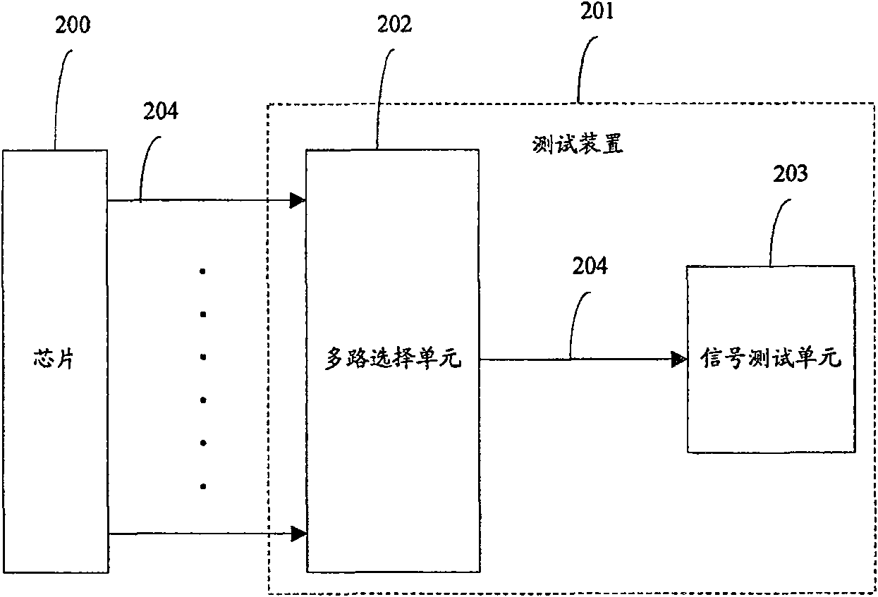
[0040] In the first embodiment, the present invention tests a chip whose pins to be tested are 8 bits. According to the above description of the test device, the specific device structure in this embodiment is as follows Figure 5 As shown, the MUX with at least 8 inputs and 4 outputs is selected as the multiplexing unit, and the 8 pins to be tested of the chip are connected to the MUX in turn. Schematic diagram of the chip test method flow chart as Figure 6 shown, including the following steps:

[0041]Step 600, the pins of the chip to be tested are connected to the MUX in the test device, and the signals of the pins to be tested of the chip are input into the MUX;

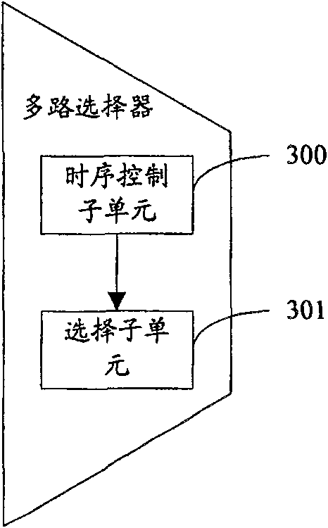
[0042] Step 601. Divide the 8-bit input pins of the MUX into two groups, the lower 4-bit MUX input pins form a group, and the upper 4-bit MUX input pins form a group. According to the number of groups, the internal timing control subunit of the MUX selects a single output signal, and the single output signal ...

Embodiment 2

[0046] In the second embodiment, the present invention also tests the chip whose pins to be tested are 8 bits. According to the description of the test device, the specific device structure in this embodiment is as follows Figure 7 As shown, the CPLD with at least 8 inputs and 4 outputs is selected as the multiplexing unit, and the 8 pins to be tested of the chip are connected to the CPLD in turn. Schematic diagram of the chip test method flow chart as Figure 8 shown, including the following steps:

[0047] Step 800, connecting the pins of the chip to be tested to the CPLD in the testing device, and inputting the signals of the pins to be tested of the chip into the CPLD;

[0048] Step 801 , after the pin signal of the chip to be tested is connected to the input terminal of the CPLD in the test device, the internal logic function of the CPLD is constructed by user-defined. In this embodiment, it is necessary to test a chip with 8-bit pins to be tested, and the signal test...


PUM


Abstract

This invention discloses one chip test method and its device, which comprises the following steps: receiving chip to be tested leg signal; selecting different leg signal from the leg signals in different time; testing the leg signal for selected one. This invention discloses one chip test device, which adopts the method to improve work efficiency and to simplify the work complexity.

Description

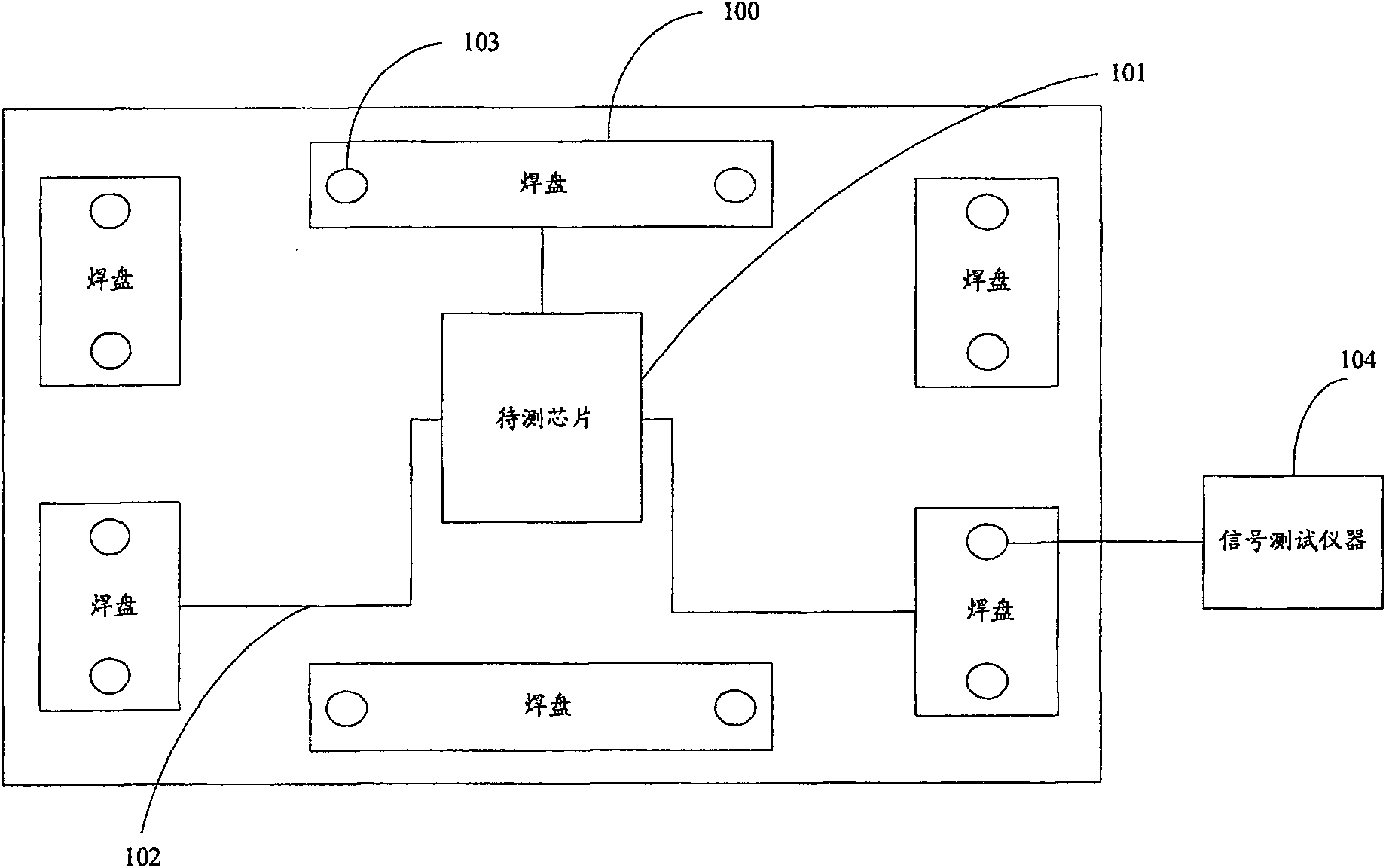
technical field [0001] The invention relates to the field of integrated circuit testing, in particular to a method for realizing chip testing. Background technique [0002] With the development of electronic technology, there are more and more types of chip packaging. In order to ensure the quality of the chip, it is often necessary to perform multiple functional tests on the chip. For chips in different packages, a test that can test chips in different packages is designed. programs are particularly important. [0003] The prior art designs a test chip circuit board, fixes the chip on the test chip circuit board, and then connects the power supply, signal test instrument and necessary electronic components used in the test to form a complete test chip device. Test the chip under test. The package form of the chip to be tested selected in the prior art is SOT23-3, and its pin quantity is three, as figure 1 The shown chip testing device includes the following parts: [00...

Claims


Application Information

Patent Timeline
Patent Type & Authority Patents(China)
IPC IPC(8): G01R31/01G01R31/28G01R1/04
Inventor 吴大畏
Owner VIMICRO CORP
Learn More