Encapsulation base plate

A technology for encapsulating substrates and circuit boards, which is applied to printed circuit components, electrical components, and electrical solid devices, and can solve problems such as warping and deformation of thinner substrates, smaller thickness of thinner substrates, and inability to meet the process. Achieve the effect of increasing strength, not easy to warp and deform, and improving bending

Active Publication Date: 2010-01-20
UNIMICRON TECH CORP
View PDF8 Cites 0 Cited by
  • Summary
  • Abstract
  • Description
  • Claims
  • Application Information

AI Technical Summary

Problems solved by technology

[0004] However, due to the reduced thickness of the thinned substrate, it cannot provide enough support to meet the requirements of planarization
Especially during high-temperature ball planting, the warping and deformation of the thinned substrate due to heating is more serious, which cannot meet the technical requirements

Method used


Image

  • Encapsulation base plate
  • Encapsulation base plate

Examples


Embodiment Construction

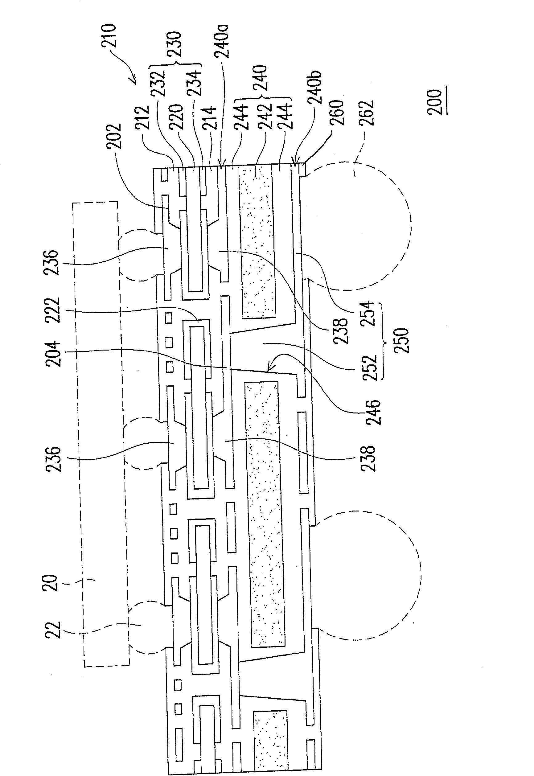
[0044] Please refer to figure 2 , which shows a schematic diagram of a package substrate according to an embodiment of the present invention. The packaging substrate 200 includes a circuit board 210 , which meets the circuit density and thickness restrictions required by the thinned substrate, so as to accelerate the transmission speed of electronic signals. The circuit board 210 has a plurality of upper contacts 202 (ie second contacts), which correspond to the bumps 22 on the connection chip 20 (indicated by dotted lines) to transmit electronic signals. In particular, the present invention uses the insulating layer 220 without glass fiber cloth and the metal layers on both surfaces to make the inner layer circuit 230, and the inner layer circuit 230 includes an upper layer circuit 232 and a lower layer circuit 234, which can be passed through the insulating layer. The plated through hole 222 of 220 is electrically connected. Wherein, the thickness of the insulating layer ...


PUM


Abstract

This invention provides a package base board including a CB, an intensified board and at least one conduction channel, in which, the intensified board is matched on the CB to resist against warp of the CB, the intensified board includes an aperture and the CB corresponds to a first connecting point exposed in the aperture, besides, one end of the conduction channel is placed in the aperture and connected to the first connecting point and the other end is placed at the second surface of the board to form a joint pad.

Description

technical field [0001] The present invention relates to a packaging substrate, and in particular to a packaging substrate capable of strengthening the structural strength of thin circuit boards. Background technique [0002] In recent years, with the rapid development of electronic technology and the emergence of high-tech electronic industries, electronic products with more humanization and better functions are constantly being introduced, and are designed towards the trend of light, thin, short and small. [0003] Please refer to figure 1 , which shows a schematic diagram of a conventional packaging substrate. In order to increase the strength of the package substrate 100 , the package substrate 100 uses a copper foil substrate 120 including glass fiber and epoxy resin as the core layer 110 to make inner layer circuits. The thickness of the copper foil substrate can reach 400-800 microns, and the required circuit layers 122 and 124 are formed by patterned etching on the ...

Claims


Application Information

Patent Timeline
Patent Type & Authority Patents(China)
IPC IPC(8): H01L23/498H05K1/02
CPCH01L2224/10H01L2924/15311
Inventor 郑振华
Owner UNIMICRON TECH CORP
Why Eureka
Try Eureka