

Sample hold circuit, and pipeline ad converter using the circuit
A technology of sampling and holding circuits and sampling capacitors, which is applied in the direction of analog-to-digital converters, analog/digital conversion, analog/digital conversion calibration/testing, etc., can solve problems such as fluctuations and narrow output dynamic ranges, and reduce power consumption and reduce The effect of operating average current
- Summary
- Abstract
- Description
- Claims
- Application Information
AI Technical Summary
Problems solved by technology
Method used
Image

Examples
Embodiment 1
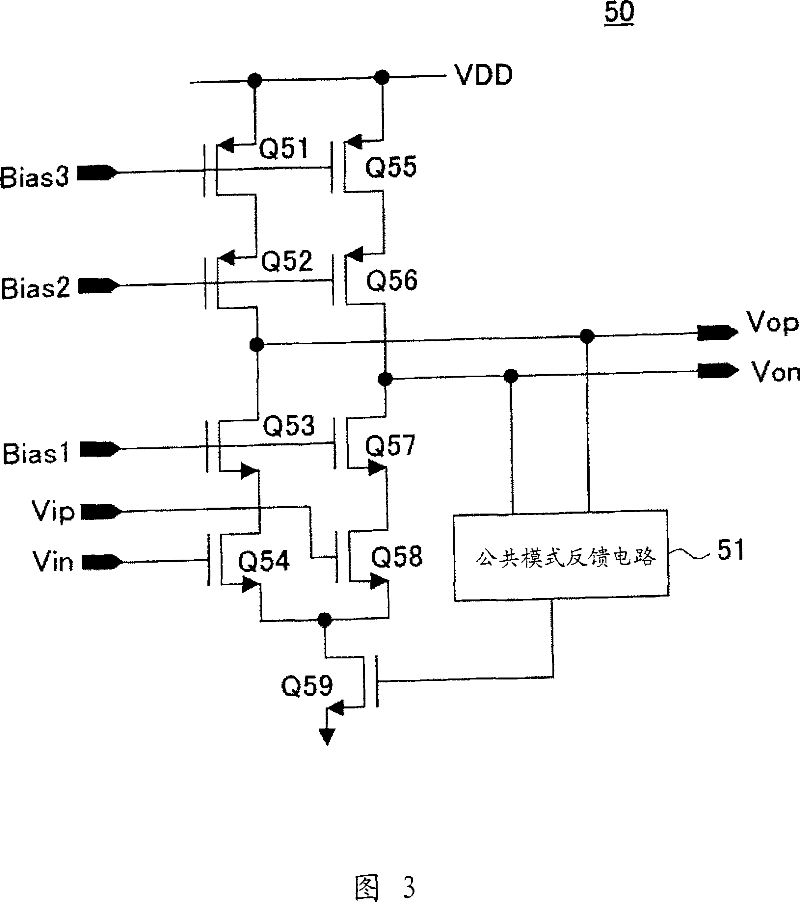
[0076] In FIG. 5 a sample and hold circuit 50 according to the invention is shown.
[0077] One side of the current source I151 is connected to the voltage source VDD, the other side is connected to the drain of the NMOS transistor Q151, and the current source I153 and the switch SW163 connected in series are connected in parallel to the current source I151. The current source I153 is a current source for flowing n times the current of the current source I151. The source of the NMOS transistor Q151 is grounded, and the SW156 is connected between the gate and the drain. Connect SW157 and capacitor Cf151 connected in series to it in parallel. The common connection point of these capacitors Cf151 and SW157 is connected to Vag via SW155.
[0078] In parallel with the NMOS transistor Q151 configuring the pseudo-differential circuit, a source-grounded NMOS transistor Q153 is provided, the gate of which is commonly connected to the gate of Q151, and the drain connected to the drain...
Embodiment 2
[0107] Next, a sample and hold circuit 200 as another embodiment of the present invention is shown in FIG. 7 . Elements of the same configuration as those of FIG. 5 are denoted here with the same reference numerals. Also, this sample hold circuit 200 has a configuration obtained by adding a common mode feedforward (CNFF) circuit to a circuit formed by deleting a part of FIG. 5 .
[0108] In the following, to simplify the circuit configuration and its description, only one MOS transistor is shown as a source-grounded transistor, but other MOS transistors can be connected in parallel by using switches, and switches (SW ) and current source.
[0109] The input of CMFF circuit 202 is connected to Vip and Vin, and is also connected to Vag. The output terminal of the CMFF circuit 202 is connected to a common connection point of capacitors Cf151 and SW157 and a common connection point of capacitors Cf152 and SW159 via SW155 and SW160 . Other circuit configurations are the same as ...
Embodiment 3
[0124] FIG. 8 shows the CMFF circuit 250 of this embodiment. The CMFF circuit 250 corresponds to the CMFF circuit 202 configured in the sample hold circuit 200 explained earlier. Timings for explaining its operation are shown in FIG. 9 . The clock signal ( CK3 , CK4 ) supplied to the CMFF circuit 250 ( 202 ) operates as an inverted clock of the control clock signal ( CK1 , CK2 ) of the sample-and-hold circuit 200 .
[0125] In FIG. 8, the input terminal supplied with Vin is connected to one end of SW251, and the other end of SW251 is connected to capacitor CS250. In addition, the common connection point of this SW251 and capacitor CS250 is connected to Vag via SW253.
[0126] The input terminal supplied with Vip is connected to one end of SW252, and the other end of SW252 is connected to capacitor CS251. In addition, the common connection point of this SW252 and capacitor CS251 is connected to Vag via SW254.
[0127] The other ends of the capacitors CS250 and CS251 are con...
PUM
 Abstract
Description
Claims
Application Information