Semiconductor device

A semiconductor and transparent technology, applied in semiconductor devices, semiconductor/solid-state device components, radiation control devices, etc., can solve the problems of light diffuse reflection, blur, abnormality, etc., and achieve high reliability effects

Inactive Publication Date: 2007-09-26
FUJITSU MICROELECTRONICS LTD
View PDF4 Cites 8 Cited by
  • Summary
  • Abstract
  • Description
  • Claims
  • Application Information

AI Technical Summary

Problems solved by technology

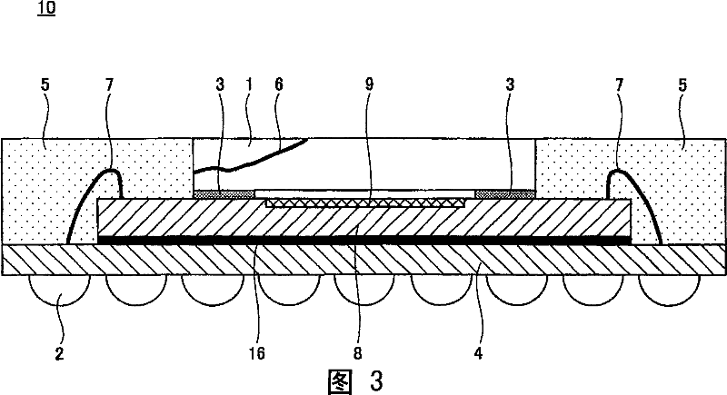
Due to this, diffuse reflection of light may occur, and thus, abnormalities such as blur (flare) may occur in the image formed on the imaging area.
In addition, due to the extension of the crack, it is possible to damage the transparent member 1 such as glass

Method used


Image

  • Semiconductor device
  • Semiconductor device
  • Semiconductor device

Examples


no. 1 example

[0086] A first example of a method of manufacturing the solid-state image sensing devices 20 , 30 , and 40 will be discussed with reference to FIGS. 11 to 14 .

[0087] Here, FIGS. 11 to 14 provide a first view to a fourth view for illustrating a first example of a method for manufacturing a solid-state image sensing device according to an embodiment of the present invention. In the following description, an example of a manufacturing method of the solid-state image sensing device 20 is discussed.

[0088] Referring to FIG. 11-(a), a transparent plate 210 formed of a rectangular glass plate is cut with a cutting blade 50 having a width (edge ​​thickness) of approximately 0.05 mm to 0.2 mm, thereby forming groove forming portions 26 . The cutting blade 50 used in this process is the same as that used in the cutting process of the transparent plate 210 shown in FIG. 11-(b).

[0089] Referring to FIG. 5 , a plurality of groove forming portions 26 are formed near the four sides o...

no. 2 example

[0101] Referring to FIG. 15 , a second example of a method of manufacturing a solid-state image sensing device will be discussed.

[0102] Here, FIG. 15 is used to illustrate the second example of the manufacturing method of the solid-state image sensing device according to the embodiment of the present invention.

[0103] While the groove forming portion 26 is formed in the transparent plate 210 by using the dicing blade 50 in the first example of the manufacturing method of the solid-state imaging sensor device 20, the groove forming portion 26 is formed by etching in the second example. .

[0104] As shown in FIG. 15-(a), a resist 60 is applied on the surface of the transparent plate 210. Referring to FIG. In addition, a portion of the groove forming portion 26 should be formed by the process shown in FIGS. 15-(b) and 15-(c) to be exposed so as not to be covered. That is, for the position where the groove forming portion 26 has a width of about 0.05 to 0.2 mm, the corresp...


PUM


Abstract

A semiconductor device includes a semiconductor element having an upper surface where an imaging area is formed; a transparent member separated from the semiconductor element by a designated distance and facing the semiconductor element; and a sealing member configured to seal an edge part of the semiconductor element and an edge surface of the transparent member; wherein a groove forming part is formed in the transparent member, the groove forming part being situated at an edge surface side of the transparent member outside of an external edge of the imaging area of the semiconductor element.

Description

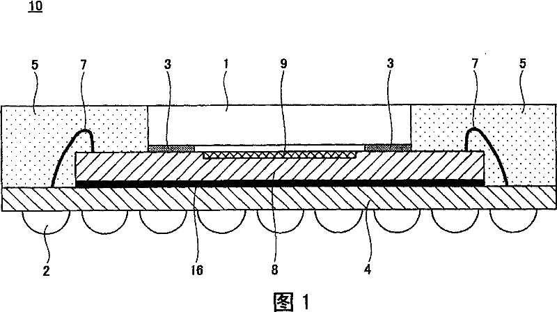
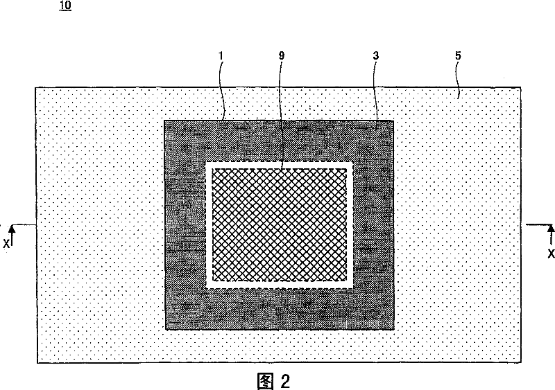
technical field [0001] The present invention generally relates to a semiconductor device, and more particularly, to a semiconductor device having a transparent member. Background technique [0002] There is known a solid-state image sensing device formed by encapsulating and modularizing a solid-state image sensor with a transparent member such as glass, a circuit board, wiring connecting the solid-state image sensor and the circuit board, sealing resin, and other parts And formed. Here, the solid-state image sensing device is, for example, an image sensor such as a Charge Coupled Device (CCD) or a Complementary Metal Oxide Semiconductor (CMOS). [0003] FIG. 1 is a cross-sectional view of a conventional solid-state image sensing device. FIG. 2 is a top view of a solid-state image sensing device in the prior art. FIG. 1 is a sectional view taken along line X-X of FIG. 2 . [0004] Referring to FIGS. 1 and 2, in the structure of a solid-state image sensing device 10, a so...

Claims


Application Information

Patent Timeline
Patent Type & Authority Applications(China)
IPC IPC(8): H01L27/14H01L23/00H01L23/02H04N5/335
CPCH01L27/14636H01L24/97H01L2924/01023H01L2924/1815H01L2924/16195H01L2924/16235H01L24/48H01L2224/97H01L2924/12041H01L2224/48227H01L2924/01005H01L2924/01033H01L2924/01006H01L2924/15311H01L2924/01078H01L27/14618H01L2924/01075H01L2224/48091H01L2224/73265H01L24/31H01L2224/32225H01L24/73H01L2924/181H01L2924/00014H01L2224/85H01L2224/83H01L2924/00H01L2924/3512H01L2924/00012H01L2224/45099H01L2224/45015H01L2924/207H01L27/146H01L27/14
Inventor 森屋晋
Owner FUJITSU MICROELECTRONICS LTD
Why Eureka
Try Eureka