Lead frame chip-level encapsulation method

A chip-level packaging and lead frame technology, applied in semiconductor devices, semiconductor/solid-state device manufacturing, electrical components, etc., to achieve the effect of low height, high stability and good heat dissipation

Inactive Publication Date: 2007-10-17
TITLE MAX TECH
View PDF0 Cites 18 Cited by
  • Summary
  • Abstract
  • Description
  • Claims
  • Application Information

AI Technical Summary

Problems solved by technology

The disadvantage is that the gull-wing pins extend beyond the encapsulant, so there is considerable room for improvement in both height (usually around 1.27mm) and width (usually around 9.22mm)

Method used


Image

  • Lead frame chip-level encapsulation method
  • Lead frame chip-level encapsulation method
  • Lead frame chip-level encapsulation method

Examples


Embodiment Construction

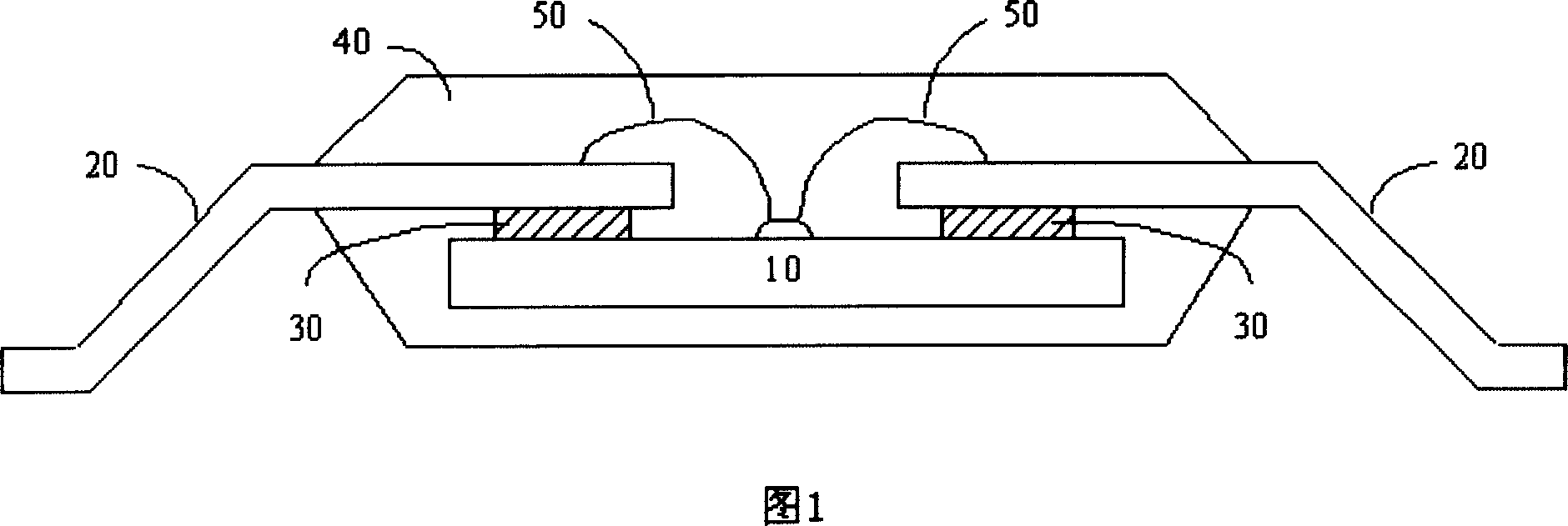
[0021] The invention provides a lead frame type chip level packaging method. This method is roughly similar to the traditional LOC process, but there are significant differences in some steps. Hereinafter, this specification will mainly describe the differences, and the same parts as those in the prior art will not be repeated.

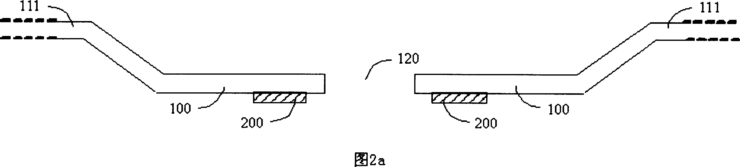
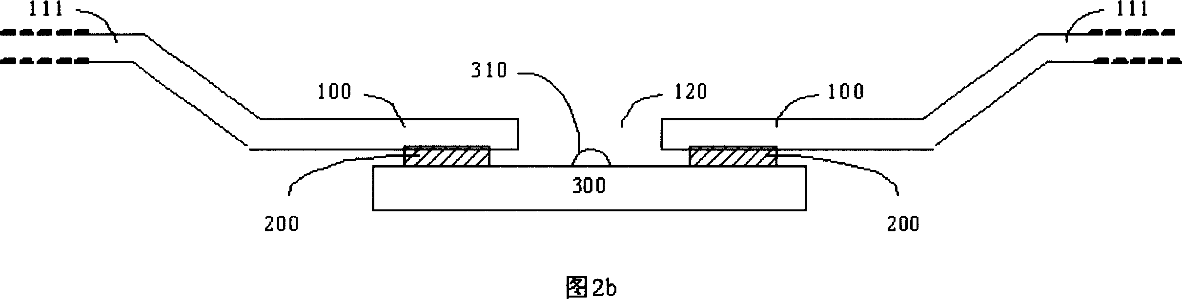
[0022] In the first step of the method, a suitable lead frame 100 is provided as shown in Figure 2a. This lead frame can be customized according to different applications after packaging. It is characterized in that the multiple pins (including internal pins 110 and external pins 111 ) of the lead frame 100 are at least located on opposite sides, and the lead frame 100 is located on the other side. Appropriate openings 120 are left at appropriate distances around. Chips to which the present invention is applicable have bond pads located at appropriate positions on the front side. The opening 120 is mainly to expose the soldering pads for wire bondi...


PUM


Abstract

The invention proposes a lead frame type chip packaging method. The invention is similar to a conventional chip hook, but has a main difference that an inside pin of a lead frame is bended towords a side of the lead frame in addvance to form a space capable of supporting a chip and a lead, while an outside pin is directly exposed under a packaging colloid, and the outside pin is not bended and shaped when removing the frame. In addition, the packaged chip of the invention is face-down positioned on the lead frame, and the lead is connected to the lead frame via an opening of the lead frame by a solder pad positioned at a face of the chip, thereby the lead is under the lead frame. Another characteristic of the invention is that, after packaging, extravasated colloid or waste colloid are removed in a laser manner but only in a mechanical die or an electrolytic manner.

Description

technical field [0001] The invention relates to a method for chip level packaging, in particular to a method for lead frame type chip level packaging. Background technique [0002] As various electronic products become increasingly complex and thinner, smaller and smaller, in order to cope with this trend, so-called chip size packages or chip scale packages (chip scale packages, CSPs) have also been widely used in chip packaging. According to the definition of IPC (Interconnecting and Packaging electronic Circuit) of EIA (Electronic Industries Association), chip-scale packaging refers to a package in which the area of ​​the sealing body after packaging is less than 1.2 times the size of the chip, and can be directly processed by surface mount technology (direct surface mountable). [0003] There are many forms of chip-level packaging, which can generally be classified into (1) substrate-based chip-level packaging, which uses a rigid (rigid) or soft (flex) substrate as the su...

Claims


Application Information

Patent Timeline
Patent Type & Authority Applications(China)
IPC IPC(8): H01L21/20H01L21/56H01L21/60B29C37/00B29C37/02
CPCH01L2224/4826
Inventor 张弘立
Owner TITLE MAX TECH
Why Eureka
Try Eureka