Wafer cleaning method after chemical milling

A technology of wafer cleaning and chemical machinery, applied in the direction of chemical instruments and methods, cleaning methods using liquids, cleaning methods and utensils, etc., capable of solving problems such as BTA residues

Inactive Publication Date: 2007-10-31
UNITED MICROELECTRONICS CORP
View PDF0 Cites 27 Cited by
  • Summary
  • Abstract
  • Description
  • Claims
  • Application Information

AI Technical Summary

Problems solved by technology

[0007] Therefore, the main purpose of the present invention is to provide a wafer cleaning method after chemical mechanical polishing, to effectively solve the problem that BTA remains on the wafer surface after cleaning in the prior art

Method used


Image

  • Wafer cleaning method after chemical milling
  • Wafer cleaning method after chemical milling
  • Wafer cleaning method after chemical milling

Examples


Embodiment Construction

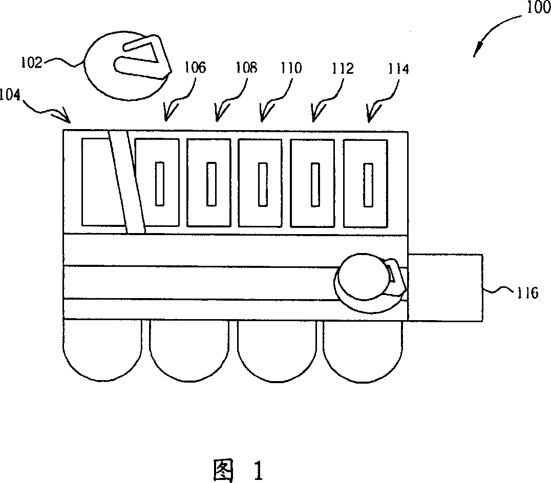
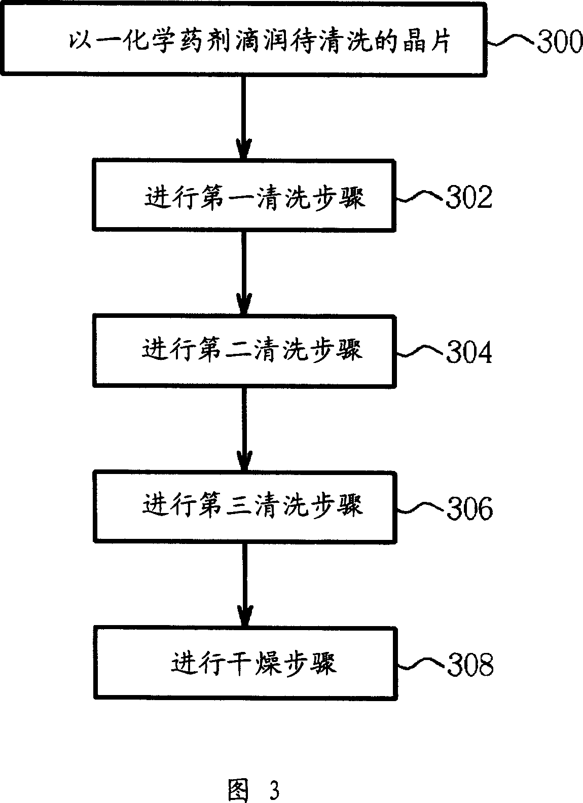
[0010] Please refer to FIG. 3, which is a flowchart of a preferred embodiment of the present invention; and please also refer to FIG. 4, which is a schematic diagram of a cleaning machine provided by a preferred embodiment of the present invention. Before cleaning the chemically polished wafer, firstly, as described in step 300 , the chemically mechanically polished wafer is placed in the buffer unit 400 of the cleaning machine for subsequent cleaning process. In step 300, chemicals are slowly dripped or sprayed on the surface of the wafer while waiting for the cleaning process to keep the surface of the wafer moist, and at the same time reduce the adhesion of BTA on the surface of the wafer, thereby preventing the wafer from waiting in the buffer unit 400 for too long Long and make the follow-up cleaning process less effective. The chemical agent can be an acidic solution such as citric acid, an alkaline solution such as an amine-containing alkaline solution, or an organic so...


PUM


Abstract

The invention relates to the wafer cleaning after chemical grinding. It loads the wafer from buffer unit to cleaning unit. Through the added chemical agent to the buffer unit, it can reduce the stickiness of the BTA surface to reduce it completely in the following process.

Description

technical field [0001] The invention relates to a wafer cleaning method after chemical grinding, in particular to a wafer cleaning method after copper chemical grinding. Background technique [0002] The Chemical-Mechanical Polishing (CMP) process is widely used in the semiconductor industry process, and is currently the most commonly used technology for global planarization of the wafer surface in the semiconductor process. The only technology that can provide comprehensive planarization of VLSI (Very Large Scale Integration, VLSI) and even Ultra Large Scale Integration (ULSI) processes. The CMP process utilizes a slurry (slurry) composed of suitable chemical additives and grinding powders, combined with the mechanical grinding applied by the grinding table, the chemical reaction provided by the chemical additives, and the mechanical interaction between the grinding powder and the wafer and the polishing pad. Grinding effect, which smoothes the uneven contours of the wafer...

Claims


Application Information

Patent Timeline
Patent Type & Authority Applications(China)
IPC IPC(8): B08B3/08B08B3/12C11D7/32C11D7/26H01L21/304
Inventor 邓清文林进坤曾佑祥梁文中
Owner UNITED MICROELECTRONICS CORP
Why Eureka
Try Eureka