

Method for producing compressive nitrifier layer and method for forming transistor
A technology of nitride layer and manufacturing method, which is applied in semiconductor/solid-state device manufacturing, electrical components, circuits, etc., to achieve the effect of increasing the contact window etching process window and improving the driving current gain
- Summary
- Abstract
- Description
- Claims
- Application Information
AI Technical Summary
Problems solved by technology
Method used
Image

Examples
no. 1 example
[0045]A method for manufacturing a compressive nitride layer according to the first embodiment of the present invention may include performing a chemical vapor deposition process, such as PECVD, to form a nitride layer on the substrate. Moreover, a specific gas needs to be introduced during the chemical vapor deposition process, and this specific gas is selected from the group including argon (Ar), nitrogen (N 2 ), krypton (Kr) and xenon (Xe) or a combination thereof. For example, when the specific gas is a combination gas of argon and nitrogen, the flow rate of the argon gas is about 100 sccm-5000 sccm, and the flow rate of the nitrogen gas is about 1000 sccm-30000 sccm. In addition, the low frequency power (LF Power) used in the chemical vapor deposition process is preferably between about 50W-3000W.
[0046] Table 1 below is a table of process parameters for using the method of the first embodiment (experimental examples 1-2) and comparing with the traditional (comparative...
no. 2 example
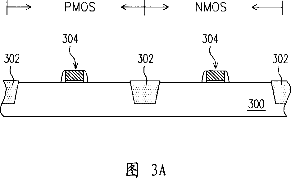
[0053] 3A to 3D are schematic cross-sectional views of a process for forming a metal-oxide-semiconductor transistor according to a second embodiment of the present invention.
[0054] Referring to FIG. 3A , a substrate 300 is firstly provided, which may have a crystal orientation on the (100) crystal plane, and it is assumed that it can be divided into a PMOS region and an NMOS region by a plurality of isolation structures 302 . And the gate structure 304 has been formed on the substrate 300 . The gate structure 304 basically includes a gate dielectric layer, a gate located on the gate dielectric layer, and a spacer formed on the sidewall of the gate. In addition, it may also include other components, but because this belongs to the scope of the present invention A person skilled in the technical field can deduce it by relying on the existing technology, so details will not be described here.
[0055] Then, referring to FIG. 3B , a source and a drain 306 are formed in the su...
no. 3 example
[0060] 4A to 4D are schematic cross-sectional views of a process for forming a metal-oxide-semiconductor transistor according to a third embodiment of the present invention.
[0061] Referring to FIG. 4A , a substrate 400 is firstly provided, which can be a substrate having a crystal orientation on the (100) crystal plane, and it is assumed that it can be divided into a first region 400a and a second region 400b by a plurality of isolation structures 402 ; For example, when the first area 400a is a PMOS area, then the second area 400b is an NMOS area. Next, a gate structure 404 is formed on the substrate 400 in the first region 400a and the second region 400b respectively. Then, the source and drain 406 are formed in the substrate 400 on both sides of each gate structure 404 , and the method of forming the source and drain 406 can refer to the description of the second embodiment (see FIG. 3B ). Afterwards, a first buffer layer (buffer layer) 408 can be optionally formed on ...
PUM
| Property | Measurement | Unit |
|---|---|---|
| Compressive stress | aaaaa | aaaaa |
| Compressive stress | aaaaa | aaaaa |
| Compressive stress | aaaaa | aaaaa |
Abstract
Description
Claims
Application Information