Nitriding method of substrate and preparation method of gallium nitride buffer layer

A gallium nitride buffer layer and substrate technology, applied in the field of microelectronics, can solve the problems of increasing the number of molecular collisions, high chamber pressure, and increasing buffer layer defects, so as to increase bombardment, expand the nitride window, and reduce the buffer layer The effect of defects

Active Publication Date: 2021-09-17
BEIJING NAURA MICROELECTRONICS EQUIP CO LTD
View PDF4 Cites 0 Cited by
  • Summary
  • Abstract
  • Description
  • Claims
  • Application Information

AI Technical Summary

Problems solved by technology

[0009] Although the above preparation method can be used to obtain a relatively smooth GaN buffer layer, however, due to the 2 o 3 The substrate has good stability, and it is difficult to break the Al-O bond when nitriding is carried out at low temperature, which leads to uneven nitriding of the substrate surface and increases buffer layer defects
However, nitriding under high temperature conditions will lead to poor growth direction of the subsequent buffer layer, which cannot effectively release stress and reduce defects.
In addition, during the epitaxial process using MOCVD equipment, a large flow of carrier gas needs to be introduced into the reaction chamber, resulting in high chamber pressure, which will increase the number of collisions of molecules and reduce the free path of molecules, thereby Inhomogeneous nitriding results in deterioration of the optical and electrical properties of the epitaxial layer

Method used


Image

  • Nitriding method of substrate and preparation method of gallium nitride buffer layer
  • Nitriding method of substrate and preparation method of gallium nitride buffer layer

Examples


specific Embodiment approach

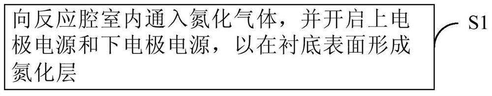
[0042] The specific implementation method of using ICP equipment to carry out nitriding treatment is as follows:

[0043] Introduce nitrogen gas into the reaction chamber, and turn on the power supply of the upper electrode and the power supply of the lower electrode. Under the action of the upper electrode power supply and the lower electrode power supply, the nitrogen gas in the reaction chamber is ionized to generate N ions and N atoms, which are accelerated, and the high-energy N ions pair Al 2 o 3 The substrate surface is bombarded, effectively opening Al-O bonds. At the same time, some N atoms and Al 2 o 3 The substrate mainly undergoes the following reactions, namely:

[0044] al 2 o 3 +N 2 →AlN+O

[0045] N atoms and Al 2 o 3 The reaction replaces Al 2 o 3 O atoms in, and in Al 2 o 3 A stable AlN layer is formed on the surface of the substrate.

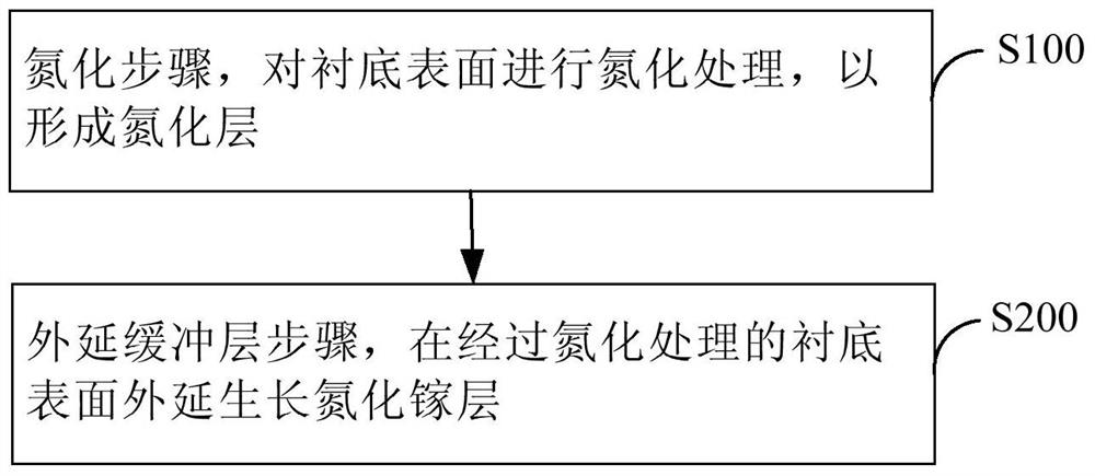
[0046] As another technical solution, figure 2 A flow chart of the preparation method of the gallium nitrid...


PUM


Abstract

The substrate nitriding method and the gallium nitride buffer layer preparation method provided by the present invention are used to use inductively coupled plasma before the epitaxial growth of the gallium nitride buffer layer and after the pattern etching of the substrate is completed The processing equipment performs nitriding treatment on the surface of the substrate, including the following steps: feeding nitriding gas into the reaction chamber, and turning on the power supply of the upper electrode and the lower electrode, so as to form a nitride layer on the surface of the substrate. The nitriding method of the substrate provided by the invention can expand the nitriding window to form a sufficient and uniform nitrided layer on the surface of the substrate, thereby reducing buffer layer defects.

Description

technical field [0001] The invention relates to the technical field of microelectronics, in particular to a method for nitriding a substrate and a method for preparing a gallium nitride buffer layer. Background technique [0002] Sapphire (A1 2 o 3 ) has become a commonly used substrate material for GaN epitaxy technology because of its mature preparation process, heat resistance, easy surface treatment, and good stability at high temperatures. However, since Al 2 o 3 There is a large lattice constant mismatch with GaN, resulting in high dislocation density in the GaN epitaxial film, so in A1 2 o 3 There will be stress in the epitaxially grown GaN film on the substrate, which will cause more dislocations and defects, and seriously affect the crystal quality of the GaN film. [0003] For this reason, the usual method for preparing GaN thin films is to etch the sapphire substrate using ICP (Inductively Coupled Plasma) etching technology, and after removing the mask, use ...

Claims


Application Information

Patent Timeline
Patent Type & Authority Patents(China)
IPC IPC(8): H01L21/02C30B25/18C30B29/20
CPCC30B25/183C30B25/186C30B29/20H01L21/0242H01L21/02458H01L21/02658
Inventor 冯林军
Owner BEIJING NAURA MICROELECTRONICS EQUIP CO LTD
Why Eureka
Try Eureka