Flat-panel display device with semi-trapezoidal tilt gate-modulated emission structure and its preparing process

A flat panel display and manufacturing process technology, applied in the manufacture of image/graphic display tubes, control electrodes, discharge tubes/lamps, etc., can solve problems such as high gate voltage, large gate current, and device damage.

Inactive Publication Date: 2007-11-14
ZHONGYUAN ENGINEERING COLLEGE
View PDF0 Cites 0 Cited by
  • Summary
  • Abstract
  • Description
  • Claims
  • Application Information

AI Technical Summary

Problems solved by technology

The control function of its gate structure is very significant, but there are unfavorable factors such as high gate voltage and too large gate current, and it is difficult to connect with conventional integrated drive circuits.
Although reducing the distance between the grid structure and the carbon nanotube cathode structure as much as possible is the most direct and easiest way to further reduce the grid operating voltage, it is also subject to the manufacturing process, insulation level, and material properties of the insulating material. Restricted by various factors, it is impossible to make the distance between the two too small, otherwise it will easily cause electrical breakdown and lead to the destruction of the whole device
Since the grid structure is located above the carbon nanotube cathode structure, it is the necessary channel for the electron beam emitted by the carbon nanotube cathode. Under the influence of the positive voltage of the grid, some electrons will inevitably be trapped by the grid structure, forming a grid structure. current, which reduces the operating current of the anode structure and reduces the brightness of the device, which is also a phenomenon that needs to be overcome
However, there is still no perfect solution to these problems

Method used


Image

  • Flat-panel display device with semi-trapezoidal tilt gate-modulated emission structure and its preparing process
  • Flat-panel display device with semi-trapezoidal tilt gate-modulated emission structure and its preparing process

Examples


Embodiment Construction

[0039] The present invention will be further described below in conjunction with the accompanying drawings and embodiments, but the present invention is not limited to these embodiments.

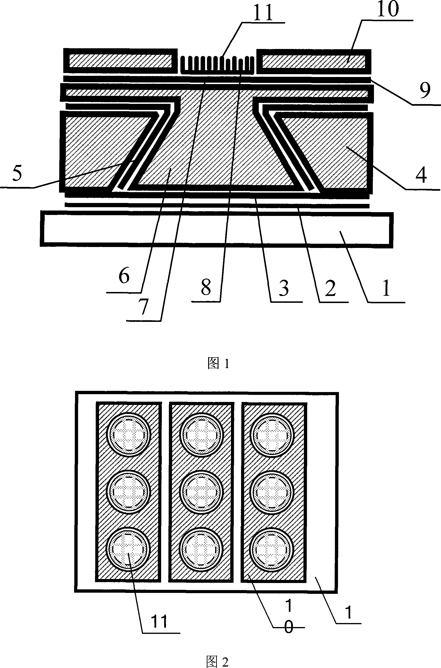
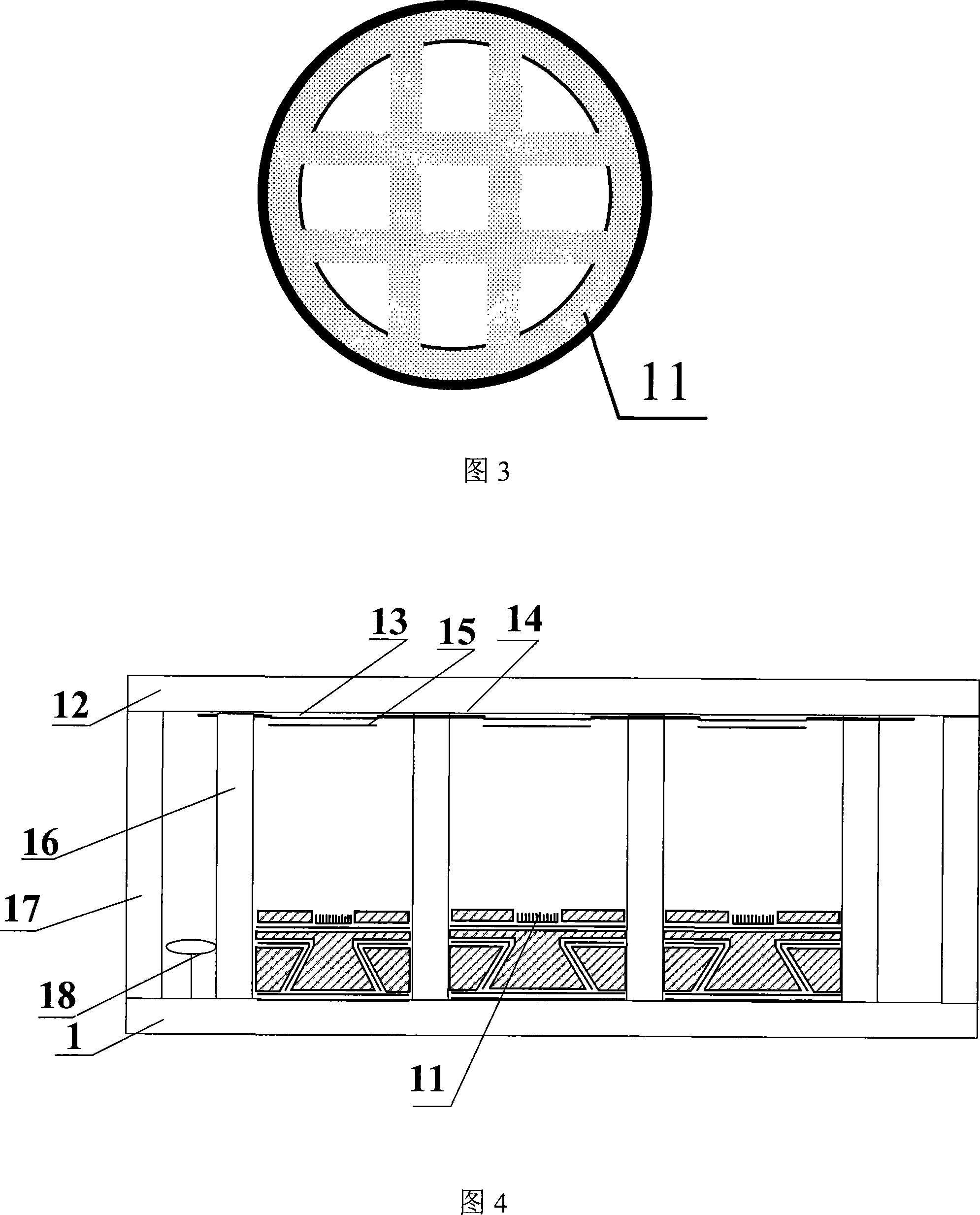
[0040] The flat panel display with a semi-trapezoidal oblique grid-controlled emission structure includes a sealed vacuum chamber formed by an anode glass panel [12], a cathode glass panel [1] and surrounding glass frames [17]; There is an anode conductive layer[13] and a phosphor layer[15] prepared on the anode conductive layer on the anode glass panel; there are cathode lead layer[9], carbon nanotubes[11] and semi-trapezoidal slanted grid on the cathode glass panel Controlled emission structure; support wall structure [16] and getter [18] accessory elements between the anode glass panel and the cathode glass panel.

[0041] The semi-trapezoidal oblique grid-controlled emission structure includes a cathode glass panel [1], an insulating layer [2], a grid lead layer [3], a grid booster layer...


PUM


Abstract

The invention relates to a flat-panel display of a semi-trapezoidal tilted grid-controlled emission structure and the making process thereof, comprising: sealed vacuum cavity composed of anode glass panel, cathode glass panel, and peripheral glass frame; anode conducting layer on the anode glass panel and fluorescent powder layer prepared on the anode conducting layer; supporting wall structure and degassing agent auxiliary component between the anode glass panel and cathode glass panel; and cathode lead layer, carbon nanotube and semi-trapezoidal tilted grid-controlled emission structure on the cathode glass panel; and it can further raise electron emission efficiency of carbon nanotube cathode, and improve whole image quality, and has advantages of stable and reliable making course, simple making process, low making cost, and simple structure.

Description

technical field [0001] The invention belongs to the fields of flat panel display technology, microelectronic science and technology, vacuum science and technology, and nano science and technology, and relates to device fabrication of flat panel field emission displays, in particular to carbon nanotube cathodes. The device production aspect of the flat panel field emission display, especially relates to a flat panel display with a semi-trapezoidal oblique grid-controlled emission structure and its manufacturing process. Background technique [0002] Carbon nanotube cathode field emission display is a solid vacuum flat display device. It uses a dot-matrix arrangement of carbon nanotube cold cathodes to emit electrons and bombard the phosphor layer to emit visible light to ensure stable and reliable display performance and bright colors. and high display image quality. Carbon nanotubes are a curly graphite layer structure with a small tip curvature radius. Under the action of ...

Claims


Application Information

Patent Timeline
Patent Type & Authority Applications(China)
IPC IPC(8): H01J31/12H01J31/15H01J29/02H01J29/04H01J1/304H01J1/46H01J9/02H01J9/00
Inventor 李玉魁
Owner ZHONGYUAN ENGINEERING COLLEGE
Why Eureka
Try Eureka