

Marking pen design for optical microscope
A technology of optical microscope and marking pen, which is applied in the direction of measuring devices, instruments, electrical components, etc., and can solve problems such as dirty structures, wrong places, and troublesome failure analysis
- Summary
- Abstract
- Description
- Claims
- Application Information
AI Technical Summary
Problems solved by technology
Method used
Image

Examples
Embodiment 1
[0052] Take the flat pen used in conjunction with the optical microscope as an example.
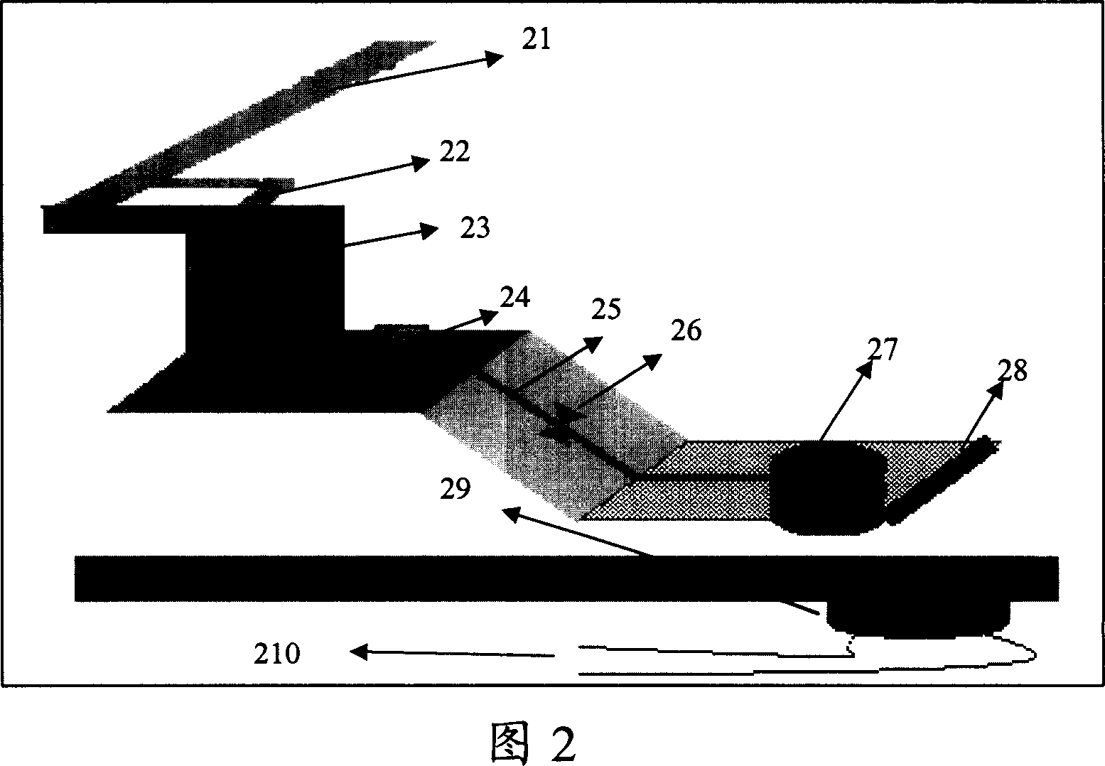
[0053] As shown in Figure 2, a fixed cantilever is led out at the head of the OM, one end of the cantilever is connected to the head of the OM, and the other end is connected to a rotatable cantilever, and a positioning baffle protrudes from the fixed cantilever near the end of the rotatable cantilever. After the rotatable cantilever rotates to a predetermined position around its connection end with the fixed cantilever, it can be blocked by the positioning baffle, so that the rotatable cantilever will not rotate too much. And position the stylus to ensure that when the cantilever is blocked by the positioning baffle, the marking ring of the stylus just entangles the light spot of the optical microscope on the wafer.
[0054] Attached to this rotatable arm is a flat-shaped marker for use with the OM. The marking pen consists of three sections, the upper and lower sections are horizontal,...
Embodiment 2
[0062] Take, for example, a flat pen used with an optical microscope.
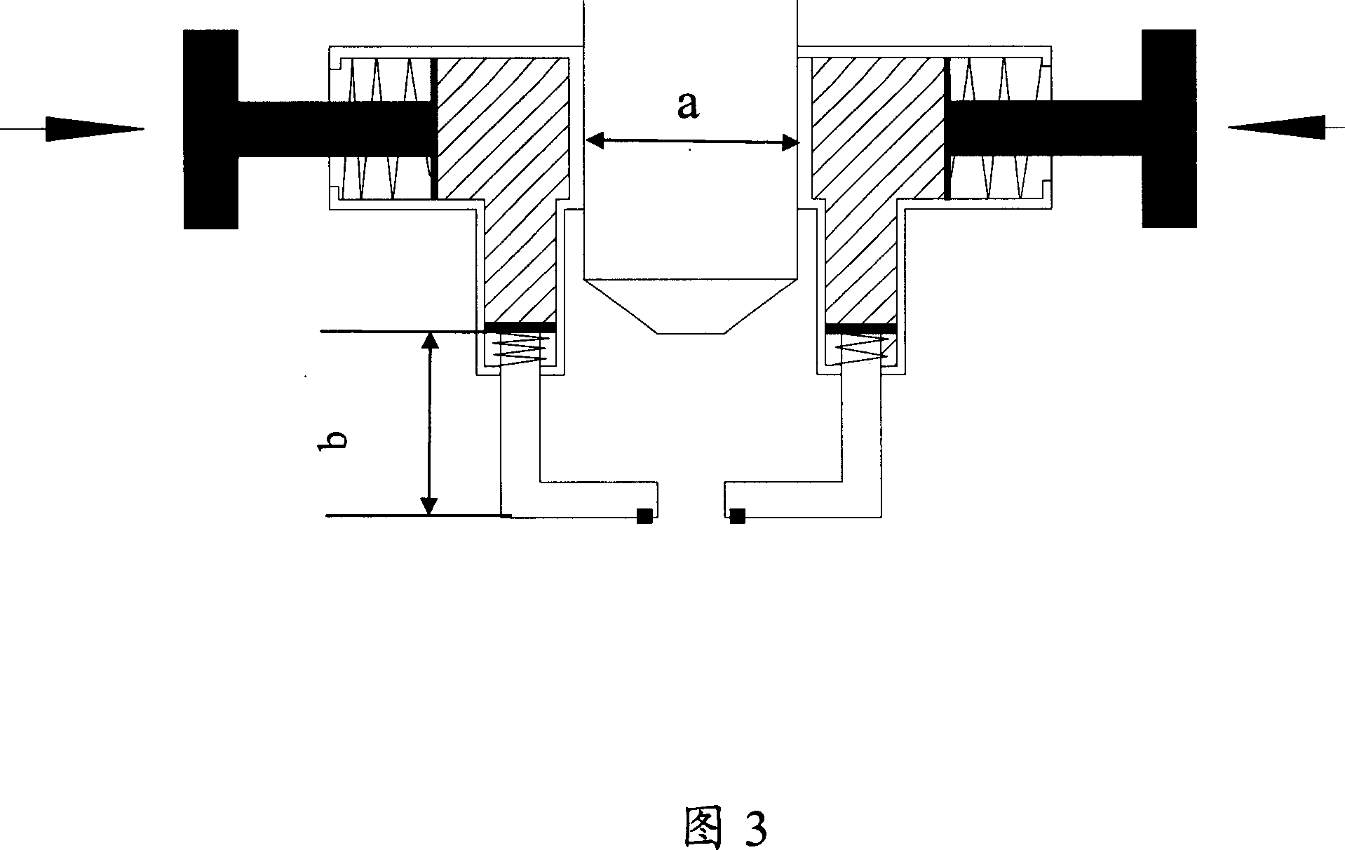
[0063] See Figure 3, the OM low magnification lens is equipped with the following piston device. The diameter a in the figure is 30 mm, which matches the diameter of the low power lens of 30 mm. The oil is in the jacket of the low magnification lens, which acts as a transmission. The marker ring is attached in the cantilever under the piston under the oil. The length of the cantilever is 12 mm, and the housing of the low power lens mentioned above is 10 mm high from the wafer, so that the marking ring can reach the wafer enough to be marked on it. And the lower power is provided with a spring for accelerating reset between the piston and the bottom of the jacket that oil is housed. The diameter of the marking ring is 8 mm, and the center of the marking ring and the center of the low-power lens are on the same vertical line, so that the marking ring can be accurately marked on the structure observed by t...
Embodiment 3
[0070] See Figure 4, put on the OM low-magnification lens a rubber coat that matches the size of the low-magnification lens, and its shape is the same as in Figure 4a.
[0071] Its cross-sectional view is shown in Figure 4b. In the figure, c is 30 mm inner diameter of the rubber jacket, matching with the 30 mm diameter of the low-magnification lens, d is 20 mm, and e is 8 mm.
[0072] When the wafer needs to be marked, the position to be marked is found with the lens through the same operation as using the OM to find the mark position when using the prior art.
[0073] When the structure to be marked in the wafer can be seen, the corresponding structure is just below the low power lens. At this time, just lower the low-magnification lens or lift the machine table to make the marking ring on the low-magnification lens contact the wafer, so as to mark the corresponding position under the lens on the wafer.
[0074] Since the rubber marking ring contacts the wafer before the lo...
PUM
 Abstract
Description
Claims
Application Information