Proctive circuit of metal-oxide-semiconductor transistor and its producing method

An oxide semiconductor and field effect transistor technology, which is applied in the field of metal oxide semiconductor field effect transistor protection circuits and their manufacturing fields, can solve problems such as abnormal curves, and achieve the effect of avoiding opening

Active Publication Date: 2007-12-05
SEMICON MFG INT (SHANGHAI) CORP +1
View PDF0 Cites 12 Cited by
  • Summary
  • Abstract
  • Description
  • Claims
  • Application Information

AI Technical Summary

Problems solved by technology

Similarly, for the LogId_Vgs_Vbs curve of a PMOS transistor with a single protection diode, when Vbs is close to zero and Vgs is greater than 0.5, the curve will be abnormal due to the forward conduction of the protection diode.

Method used


Image

  • Proctive circuit of metal-oxide-semiconductor transistor and its producing method
  • Proctive circuit of metal-oxide-semiconductor transistor and its producing method
  • Proctive circuit of metal-oxide-semiconductor transistor and its producing method

Examples


Embodiment Construction

[0033] The present invention will be further described below in conjunction with the accompanying drawings and specific embodiments.

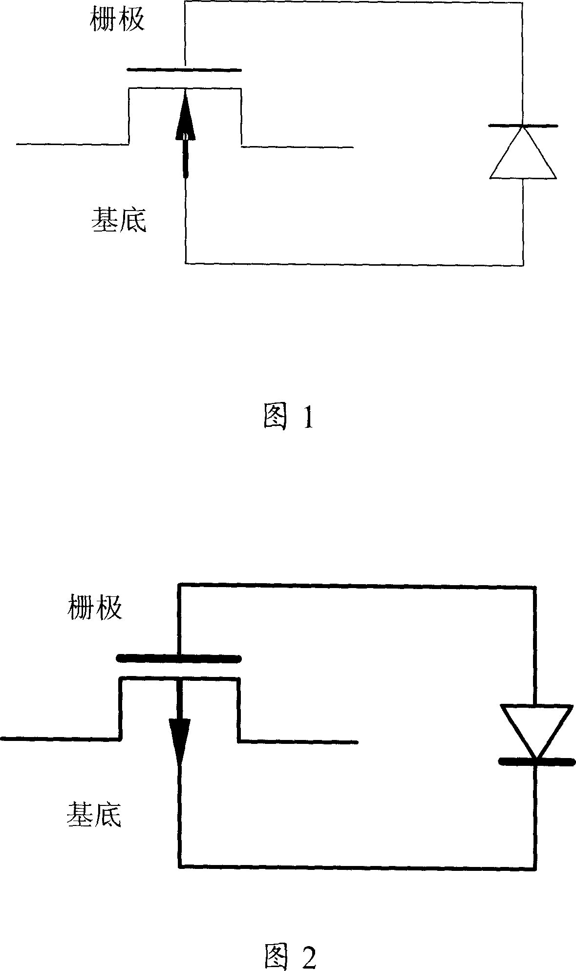
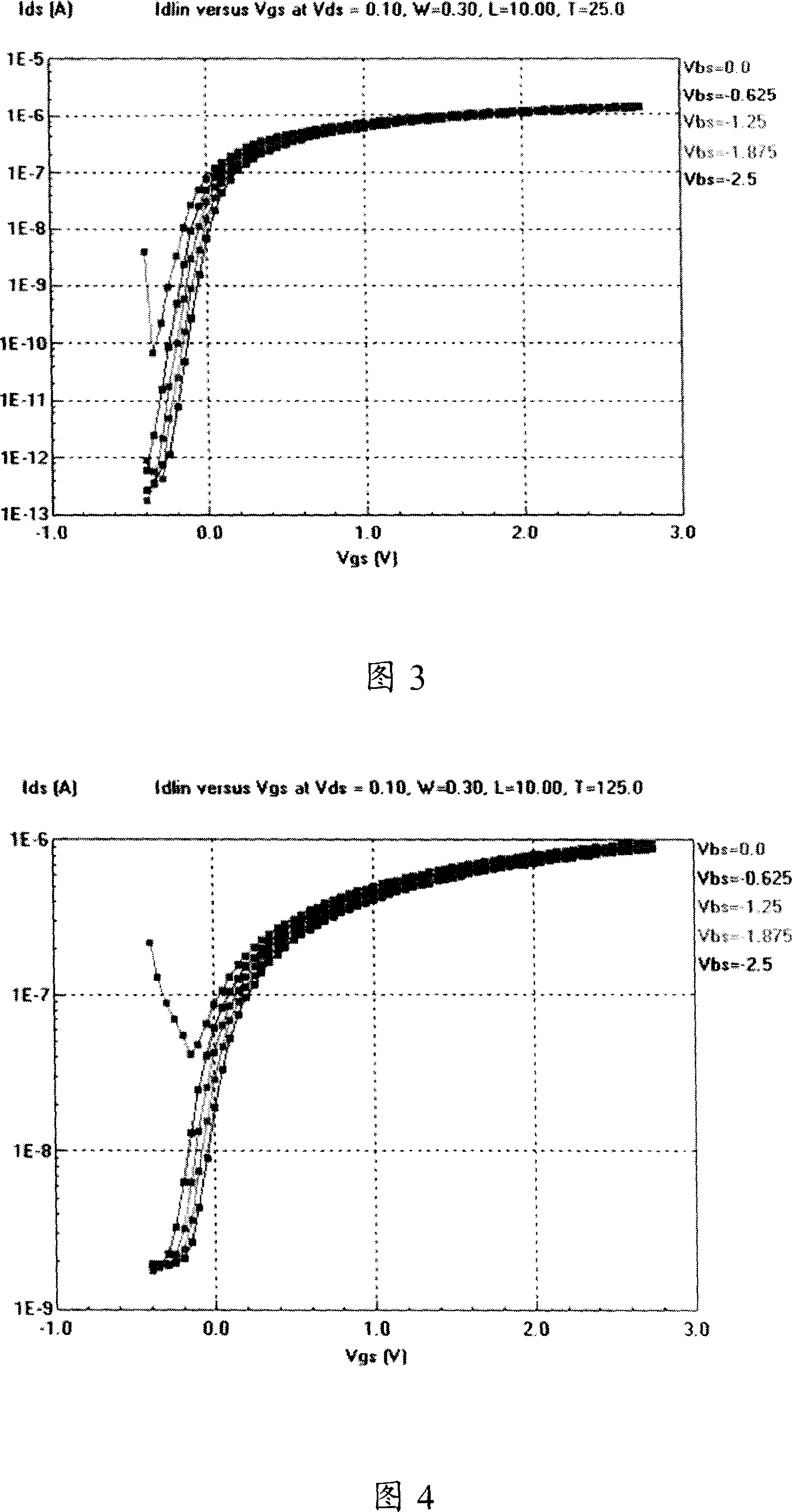
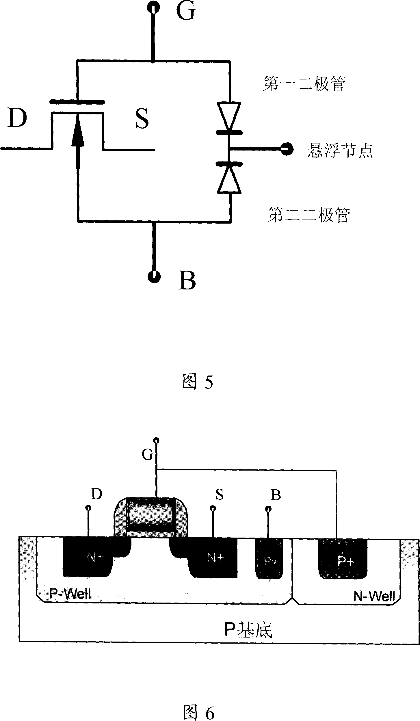
[0034] Please refer to FIG. 5 first, which is a circuit diagram of the NMOS transistor and its dual protection diodes of the present invention. In Fig. 5, in order to prevent the protection diode from being turned on, a head-to-head dual diode is designed in the present invention to protect the NMOS tube, to prevent the metal oxide semiconductor from being affected by the antenna effect at low turn-on voltage Vt and zero turn-on voltage, and to prevent the metal oxide semiconductor from being affected by the antenna effect when the turn-on voltage Vt is zero. Voltage to positive voltage measures the current-voltage characteristics of the NMOS tube, and the protection structure of its two protection diodes ensures that no leakage current that makes the diode conduction passes.

[0035] In FIG. 5 , the NMOS transistor has four connections of a so...


PUM


Abstract

The invention is a MOS field effect transistor (MOSFET) protective circuit, comprising NMOS tube and two protective diodes, where the anodes of the two diodes are connected with grid of the NMOS tube and with a substrate, respectively, and their cathodes are interconnected with each other. And it can protect MOS from being influenced by antenna effect and besides, assure the current-voltage characteristic of MOS tube is completely measured.

Description

Technical field [0001] The invention relates to the technical field of semiconductor manufacturing, in particular to a metal oxide semiconductor field effect transistor protection circuit and a manufacturing method thereof. Background technique [0002] At present, for the VLSI manufacturing industry, with the continuous reduction in the size of MOSFET (Metal Oxide Semiconductor Field Effect Transistor) devices, it is more and more important to add protection diodes to the circuit patterns of Metal Oxide Semiconductor Field Effect Transistors to avoid antenna effects . [0003] The antenna effect means that when the plasma process is used in the integrated circuit manufacturing process, there will be charges remaining on the gate metal layer, resulting in an unknown dielectric layer electric field. Due to the miniaturization of the process, the components themselves can withstand The collapse electric field is also relatively decreased, so when these residual charges are ex...

Claims


Application Information

Patent Timeline
Patent Type & Authority Applications(China)
IPC IPC(8): H01L27/04H01L21/822
Inventor 苏鼎杰黄威森萧金燕
Owner SEMICON MFG INT (SHANGHAI) CORP
Why Eureka
Try Eureka