Check patentability & draft patents in minutes with Patsnap Eureka AI!

An encapsulated chip and its encapsulation method for chip

A technology for packaging devices and chips, which is applied in the direction of semiconductor/solid-state device parts, semiconductor devices, electrical components, etc., can solve problems such as time-consuming, unfavorable FPGA modular design, inconvenience, etc., to facilitate testing and debugging, and realize The effect of visibility

Inactive Publication Date: 2008-01-09
ZTE CORP
View PDF0 Cites 7 Cited by
  • Summary
  • Abstract
  • Description
  • Claims
  • Application Information

AI Technical Summary

Problems solved by technology

It is inevitable to encounter problems during debugging and testing. At this time, it is necessary to analyze the problem. At this time, it is very likely to need to monitor the signal changes inside the FPGA. This internal signal can be passed through JTAG (Joint Test Action Group) by specific software. ) interface to capture, but this method requires re-synthesis and wiring operations on the device, which will take a lot of time and require additional FPGA internal resources to implement, which is not convenient in the case of large-scale resource constraints , which is very unfavorable to the modular design of FPGA
Another way to debug is to lead the internal signal to the temporary pin of the FPGA, because now the multi-pin FPGA basically adopts the BGA type, such as EBGA (enhanced ball grid array package), FBGA (fine pitch ball grid array package) ) and other packaging methods, the pins of the chip cannot be touched on the surface of the chip, which requires test points to be drawn out for these temporary pins, which is another limitation on PCB board-level wiring

Method used


Image

  • An encapsulated chip and its encapsulation method for chip
  • An encapsulated chip and its encapsulation method for chip

Examples


Embodiment Construction

[0032] The present invention will be further described below in conjunction with the accompanying drawings and preferred embodiments.
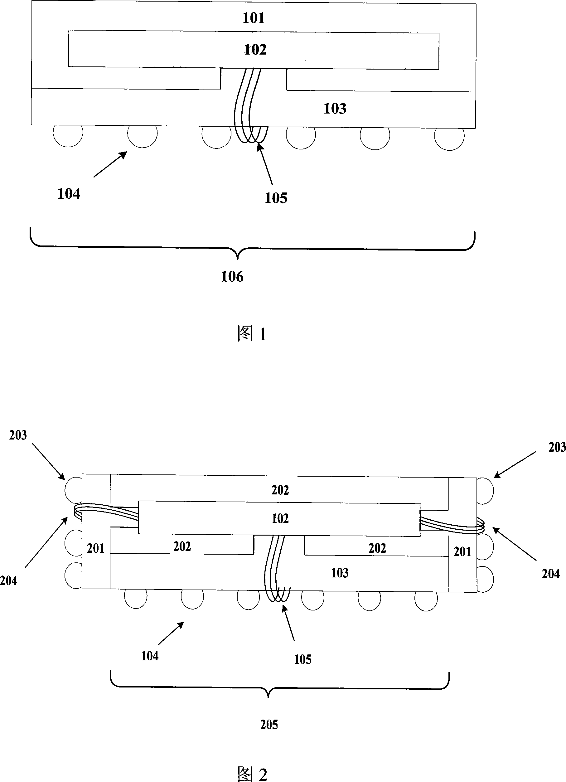
[0033] The main idea of ​​the present invention is: when the chip is packaged, the same signal pin is simultaneously led to the lower surface and the side surface of the chip for physical packaging. In this way, when using the packaged chip after packaging, if the packaged chip is soldered on the PCB (printed circuit board) to be used, the chip pins on the bottom of the soldered chip are invisible to the user. When debugging and testing the packaged chip, when the signal pin needs to be measured, it only needs to measure the exposed signal pin on the side of the chip.

[0034] Still taking BGA packaging as an example, Fig. 2 shows a BGA packaging method of a chip realized in the present invention: the packaged chip 205 includes: chip 102, substrate 103, lower surface solder ball 104, wire bridge 105, test Substrate 201, mold cap 202, side sol...


PUM


Abstract

The invention is concerned with the testing and debugging method for the packaging core plate and its packaging method. The packaging core plate includes: the core plate, the group of signal jointing foot set on the basal board which can use for educing the signal of the signal pin opposites the core plate; the packaging includes also the group of signal mount eyeble to the users, which is on the testing basal board against the signal pin of the core plate and is totally eyeable to the users. The group of eyeble signal mount achieves the visibility of core plate after it welding connects with the PCB during testing, which creates convenience for the packaging core plate testing and debugging.

Description

technical field [0001] The invention relates to the field of microelectronics and integrated circuit manufacturing, and more specifically relates to a package chip and a method for packaging the chip. Background technique [0002] In today's high-speed digital systems, due to performance requirements, there are more and more applications of ASIC (Application Specific Integrated Circuit). In high-end and high-speed systems, ASIC has its own unique advantages. It can work at a relatively high frequency , providing performance that cannot be achieved by general-purpose chips. However, ASIC also has its own shortcomings. Because it is not programmable, it is difficult to develop and maintain, especially in terms of maintenance. Even if a small function is to be added or changed, it needs to be redesigned and taped, resulting in its development cost. The geometric progression increases. Therefore, more and more FPGAs (Field Programmable Gate Arrays) are now being used to replac...

Claims


Application Information

Patent Timeline
Patent Type & Authority Applications(China)
IPC IPC(8): H01L23/544H01L23/488H01L21/60
CPCH01L2224/14
Inventor 杨焱吴兆胜李嵩潘建农
Owner ZTE CORP
Features
  • R&D
  • Intellectual Property
  • Life Sciences
  • Materials
  • Tech Scout
  • Unparalleled Data Quality
  • Higher Quality Content
  • 60% Fewer Hallucinations
Learn More