

A compensation injection method for effectively reducing LDNMOS cut-off current and avoiding dual peak feature and its application
A technology of cut-off current and characteristics, applied in the manufacturing of circuits, electrical components, semiconductor/solid-state devices, etc., can solve the problems affecting the low leakage performance of the device and the high power consumption of the device
- Summary
- Abstract
- Description
- Claims
- Application Information
AI Technical Summary
Problems solved by technology
Method used
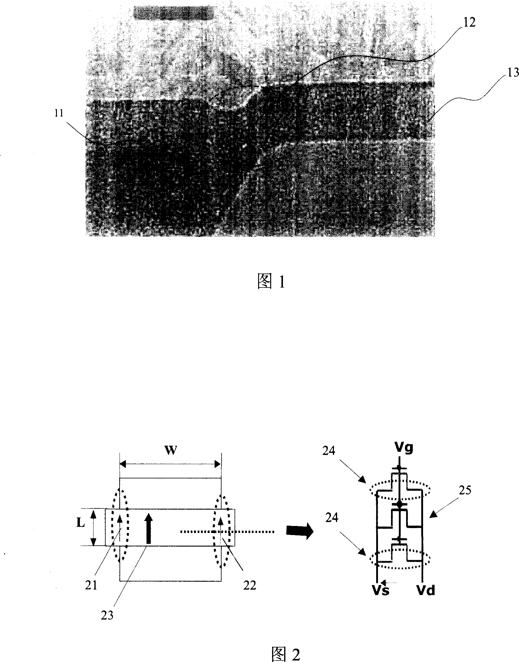
Image

Examples
Embodiment Construction
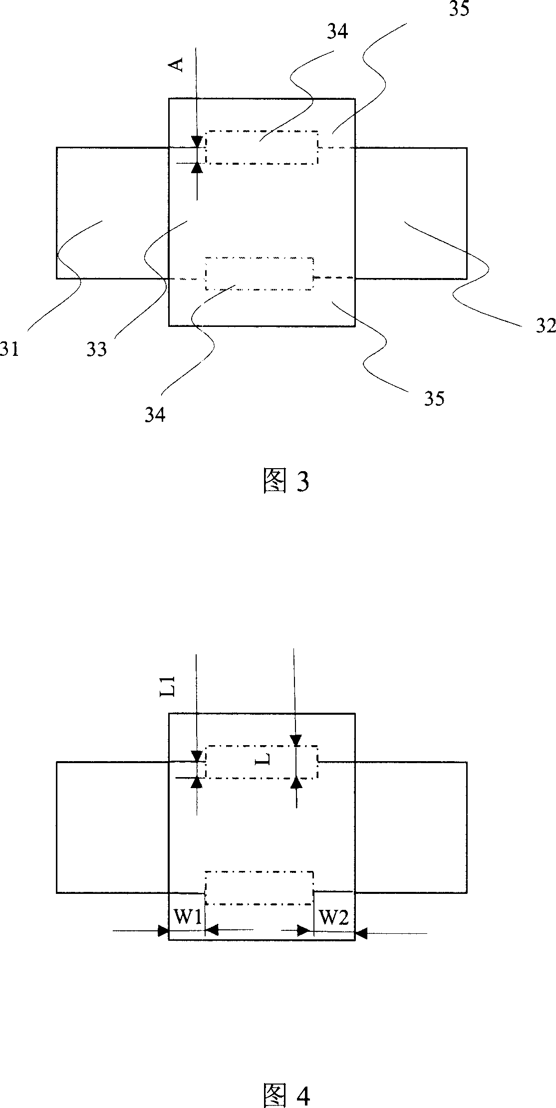
[0023] In the existing manufacturing flow of LDNMOS with channel length = 3.5um and channel width = 20um 40V, a photolithography is added after the existing triple gate (Triple Gate) process.
[0024] Specific areas are patterned on the mask used in this additional lithography.
[0025] Referring to Fig. 4, L1 in the figure is 0.2um, and L is 0.5um. W1=W2=0.5um.
[0026] After exposure and baking, B ion implantation is performed.
[0027] B ion implantation, using 20kev-50kev, B doping concentration using 10 12 -10 13 / cm 2 .
[0028] After the ion implantation, the photoresist is removed, and the subsequent LDNMOS production process is performed, and these subsequent processes are the same as the prior art.
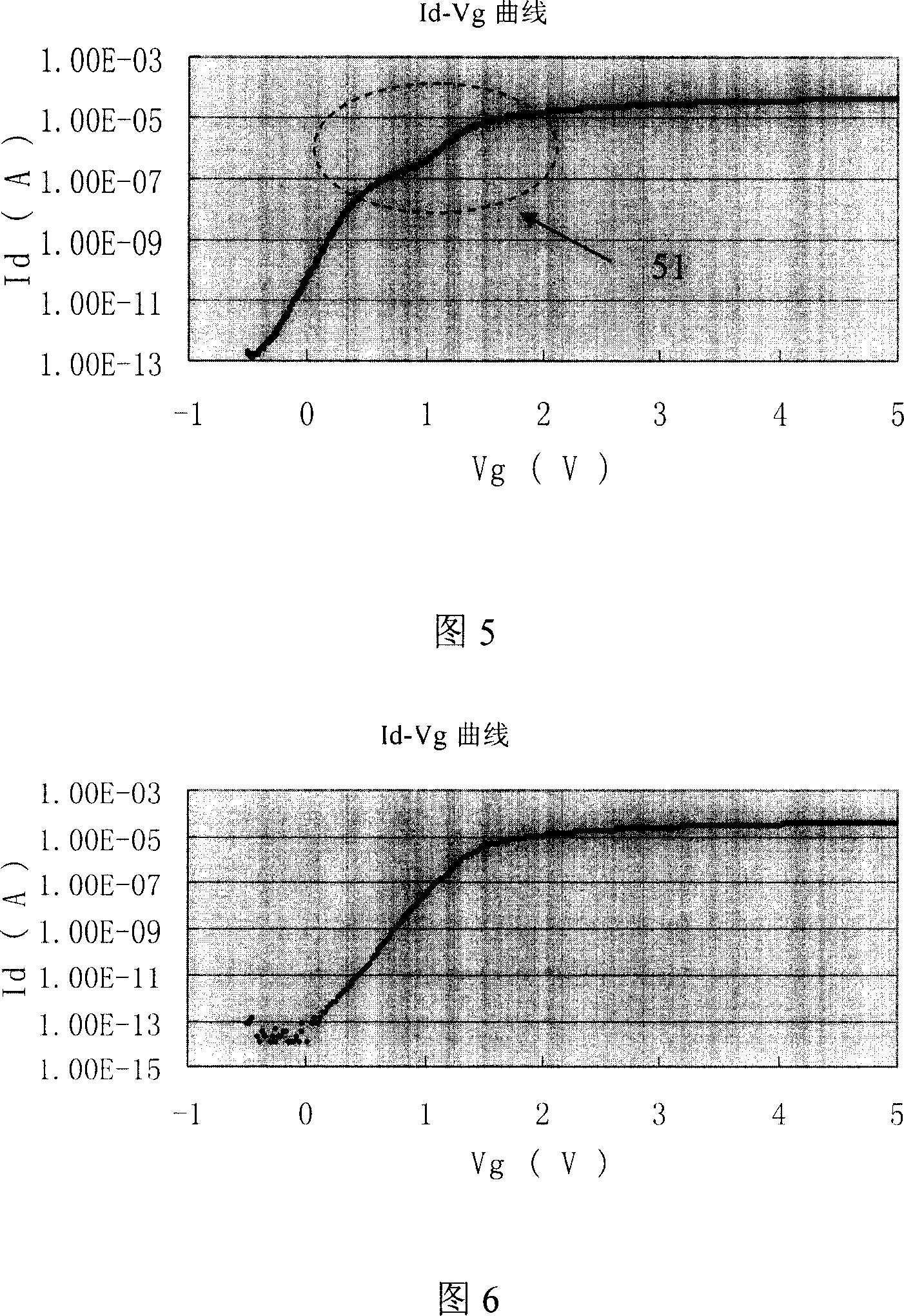
[0029] The LDNMOS transistor produced after using the embodiment is detected, and its Id-Vg characteristic curve is shown in Figure 6. When Vg=0V, Id is about 1.00E-13A / um; and in the existing transistor Id-Vg curve , the Id value when Vg=0V is about 1.00E-11A / um....
PUM
 Abstract
Description
Claims
Application Information