Non-volatile memory devices including dummy word lines and related structures and methods

A technology of non-volatile storage and virtual word lines, which is applied in the field of electronic equipment and can solve problems such as existing needs

Active Publication Date: 2008-01-16
SAMSUNG ELECTRONICS CO LTD
View PDF2 Cites 36 Cited by
  • Summary
  • Abstract
  • Description
  • Claims
  • Application Information

AI Technical Summary

Problems solved by technology

[0006] Although non-volatile memory devices are known, there remains a need for techniques that provide structures and methods of more highly integrated memory devices

Method used


Image

  • Non-volatile memory devices including dummy word lines and related structures and methods
  • Non-volatile memory devices including dummy word lines and related structures and methods
  • Non-volatile memory devices including dummy word lines and related structures and methods

Examples


Embodiment Construction

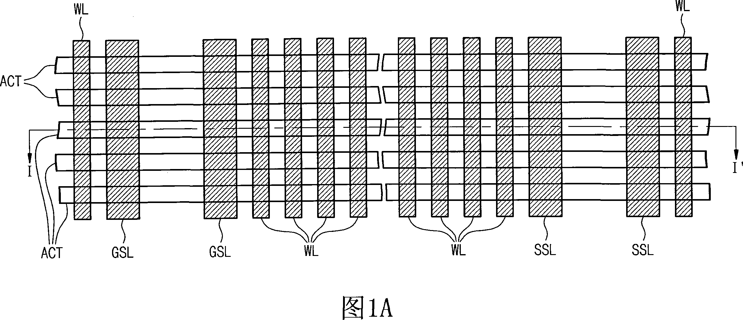
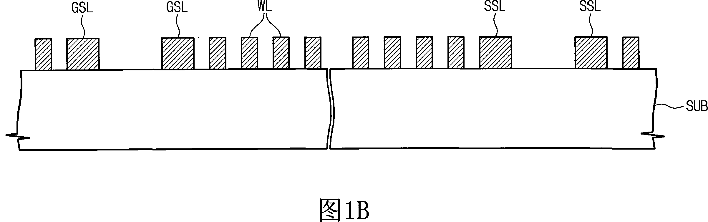
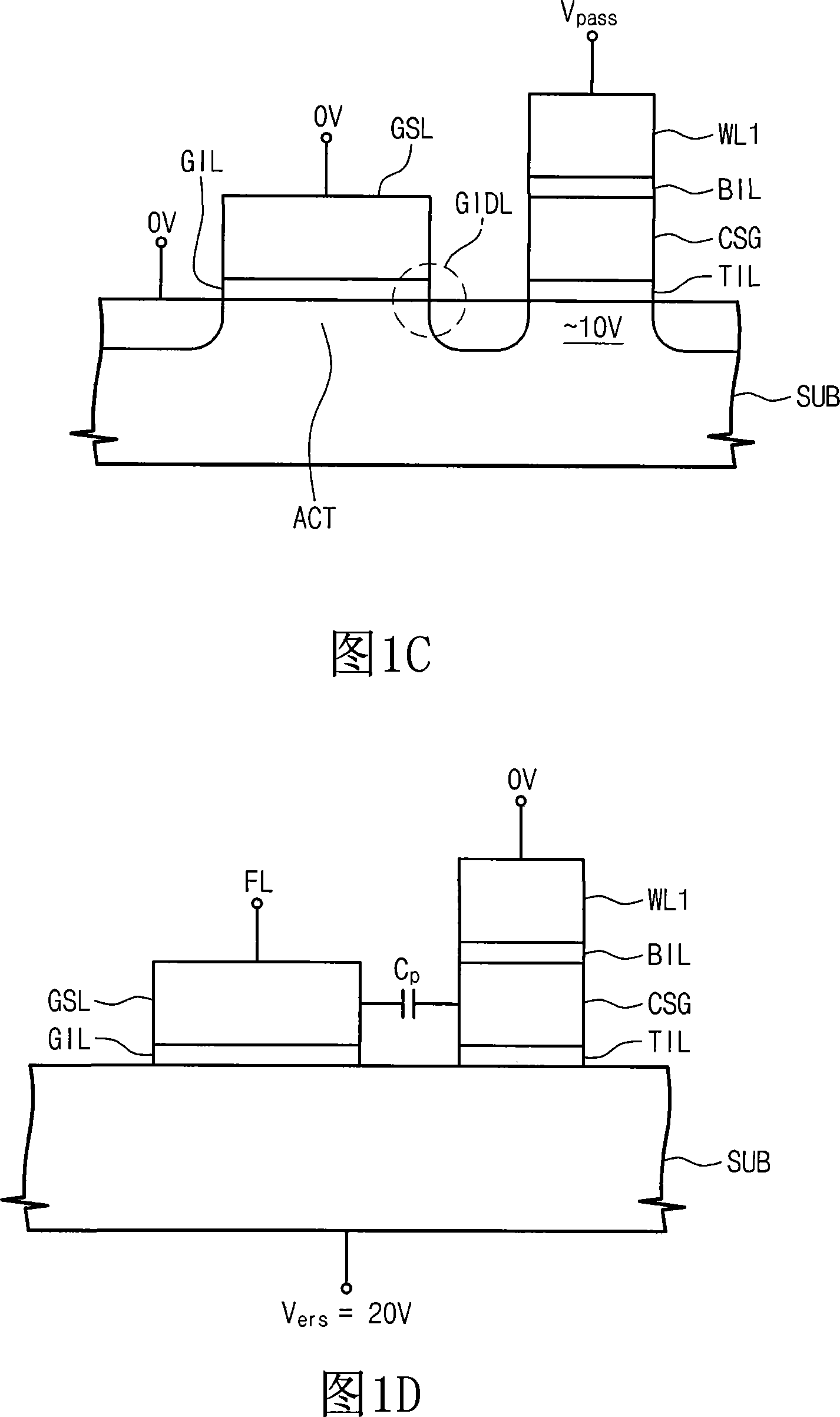
[0042] The present invention will be described more fully below with reference to the accompanying drawings, in which embodiments of the invention are shown. However, the present invention can be embodied in many different ways and should not be considered limited to the embodiments set forth herein. On the contrary, these embodiments are provided for the thoroughness and completeness of this disclosure and fully convey the scope of the present invention to those skilled in the art. In the figure, the size and relative size of layers and regions can be exaggerated for clarity. The same number always refers to the same element.

[0043] It will be understood that when an element or layer is referred to as being "on", "connected to" and / or "coupled to" another element or layer, it can be directly on the other element or layer , Directly connected or coupled to another element or layer, or intervening elements or layers may be present. In contrast, when an element is referred to as b...


PUM


Abstract

A non-volatile memory device may include a semiconductor substrate including an active region at a surface thereof, a first memory cell string on the active region, and a second memory cell string on the active region. The first memory cell string may include a first plurality of word lines crossing the active region between a first ground select line and a first string select line, and about a same first spacing may be provided between adjacent ones of the first plurality of word lines. The second memory cell string may include a second plurality of word lines crossing the active region between a second ground select line and a second string select line, and about the same first spacing may be provided between adjacent ones of the second plurality of word lines. Moreover, the first ground select line may be between the second ground select line and the first plurality of word lines, and the second ground select line may be between the first ground select line and the second plurality of word lines. Moreover, portions of the active region between the first and second ground select lines may be free of word lines, and a second spacing between the first and second ground select lines may be at least about 3 times greater than the first spacing. Related methods are also discussed.

Description

[0001] Related application [0002] According to 35 U.S.C. §119, this U.S. non-provisional patent application claims the priority of Korean Patent Application No. 10-2006-0065040 filed on July 11, 2006, so the entire disclosure is incorporated herein by reference. Technical field [0003] The present invention relates generally to electronic equipment, and more specifically to electrical storage devices and related methods. Background technique [0004] A nonvolatile memory device, such as a flash memory device, can be provided in a NOR-type structure or a NAND-type structure. For example, NOR-type flash memory devices can provide faster random access, and NAND-type flash memory devices can provide lower cost and / or higher integration. Therefore, NOR-type flash memory devices can be used for code memory storage, and NAND-type flash memory devices can be used for mass memory storage. [0005] For example, in US Patent No. 7,079,437 entitled "Nonvolatile Semiconductor Memory Device ...

Claims


Application Information

Patent Timeline
IPC IPC(8): H01L27/115H01L23/522H01L23/528H01L21/8247H01L21/768
CPCG11C16/0483G11C16/3427H10B63/80
Inventor 薛钟善崔正达朴泳雨朴镇泽
Owner SAMSUNG ELECTRONICS CO LTD
Why Eureka
Try Eureka