Mounting device for electrical component

A technology for mounting devices and electrical components, which is applied in the direction of electrical components, electrical components, and electrical components to assemble printed circuits, etc., which can solve problems such as increased misalignment, inability to fully ensure the reliability of the initial on-resistance connection, and misalignment of the IC chip substrate , to achieve the effect of preventing positional misalignment

Inactive Publication Date: 2008-01-23
DEXERIALS CORP
View PDF2 Cites 11 Cited by
  • Summary
  • Abstract
  • Description
  • Claims
  • Application Information

AI Technical Summary

Problems solved by technology

[0006] However, in such prior art, since the connection portion between the IC chip and the substrate, that is, the pressing force between the bump and the pattern is insufficient, sufficient connection cannot be made, and there is a problem that the initial on-resistance cannot be ensured sufficiently. and connection reliability issues after aging
[0007] In addition, in the method of applying pressure and heating using a thermocompression joint made of an elastic body, there is a problem that the IC chip and the substrate are misaligned during pressure bonding.
[0008] And, in this way, especially in the case of collectively mounting a plurality of IC chips, the above-mentioned misalignment tends to increase.

Method used


Image

  • Mounting device for electrical component
  • Mounting device for electrical component
  • Mounting device for electrical component

Examples


Embodiment Construction

[0038] Hereinafter, embodiments of an electrical component mounting device according to the present invention will be described in detail with reference to the drawings.

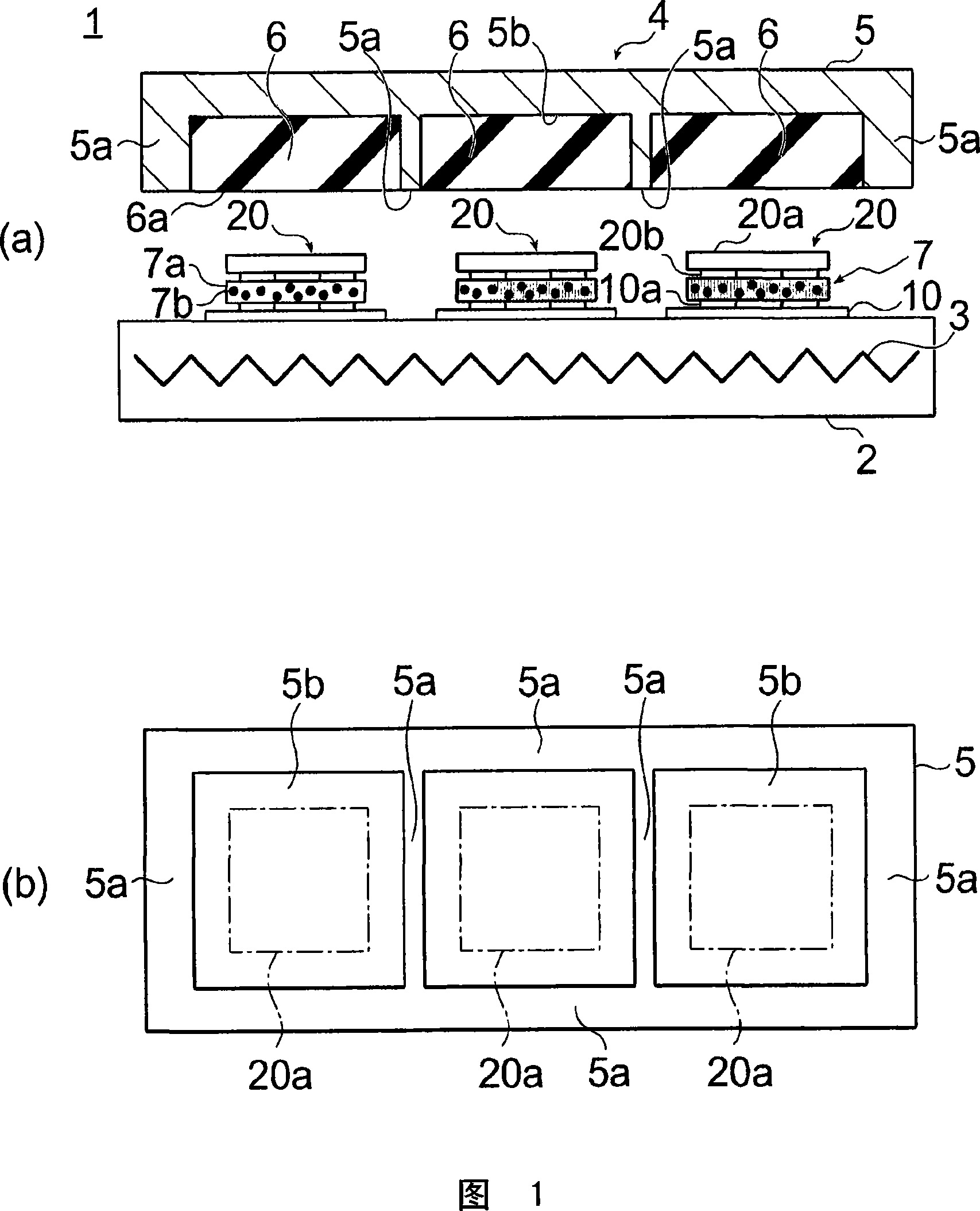
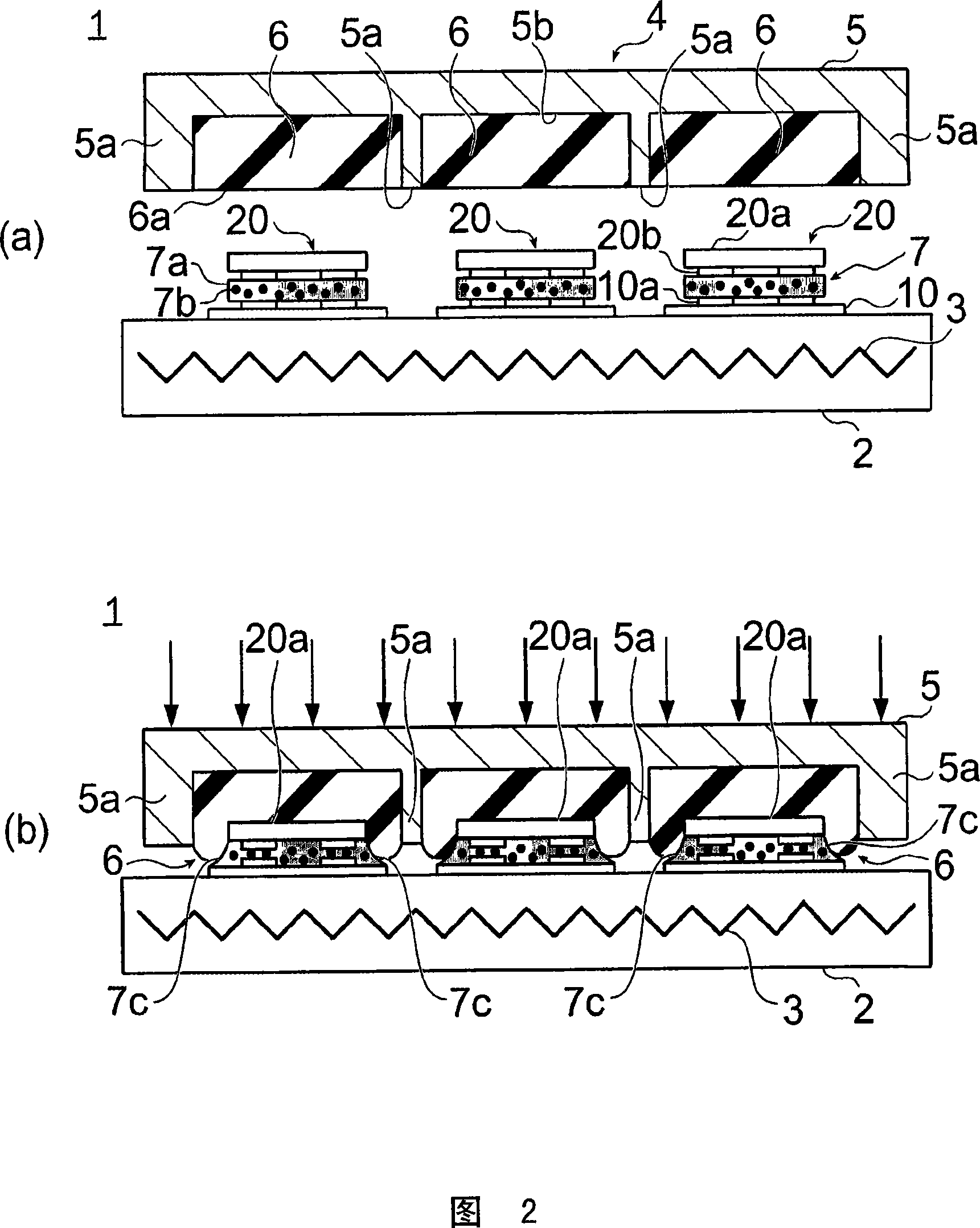
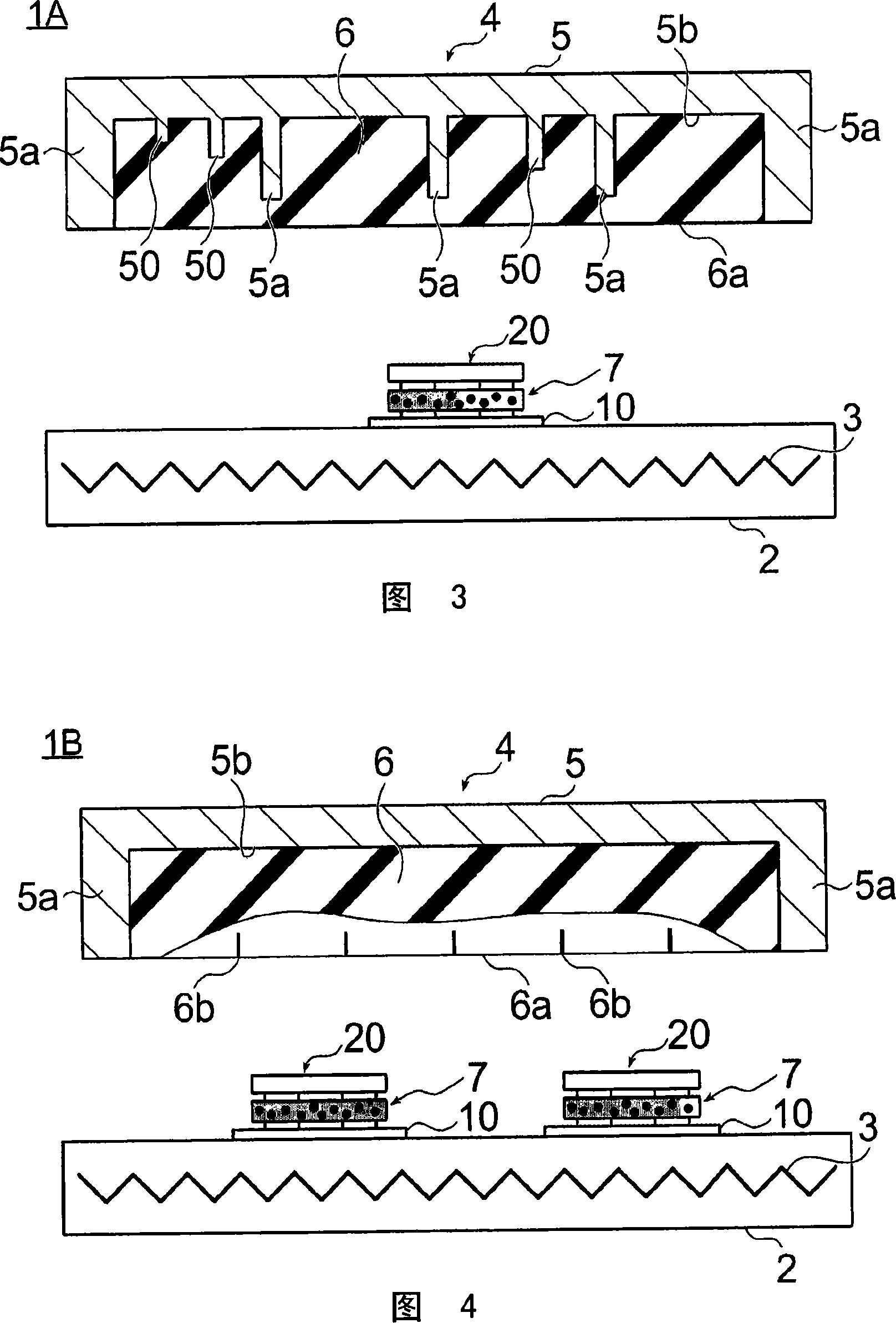
[0039] FIG. 1( a ) is a schematic configuration diagram showing a main part of a mounting device according to this embodiment, and FIG. 1( b ) is an explanatory diagram showing a positional relationship between a thermocompression joint and an IC chip of the mounting device.

[0040] As shown in FIG. 1(a) and FIG. 1(b), the mounting device 1 of this embodiment includes: a base 2 on which a wiring substrate 10 on which a wiring pattern 10a is formed is placed; and a base 2 on which a bump 20b is provided. The thermocompression joint 4 that pressurizes and heats the IC chip (electrical component) 20 .

[0041] Here, the base 2 is made of a predetermined metal, and a heater 3 for heating is provided inside it.

[0042] On the other hand, the thermocompression head 4 has a head body 5 made of a predetermined me...


PUM


Abstract

The present invention provides a mounting device capable of highly reliable mounting a plurality of electrical components using an adhesive agent. The present invention is a mounting device including a thermocompression bonding head 4 having a pressure bonding member 6 made of a predetermined elastomer provided in a head main body 5, and the mounting device is constructed such that an IC chip 20 placed on a wiring board 10 is pressed by the pressure bonding member 6 at a predetermined pressure, and further includes a pressing force adjusting mechanism for adjusting pressing force corresponding to a region on a pressure bonding surface 6a of the pressure bonding member 6. A pressing force adjusting mechanism can be used in which a plurality of pressing force adjusting frames 5a are provided in the head main body 5, and the pressure bonding member 6 is disposed inside these pressing force adjusting frames 5a.

Description

technical field [0001] The present invention relates to a technique of mounting electrical components such as semiconductor chips on a wiring substrate, and more particularly relates to a technique of mounting electrical components using an adhesive. Background technique [0002] Conventionally, as a method of directly mounting a bare chip on a wiring board such as a printed wiring board, a method using an anisotropic conductive adhesive film in which conductive particles are dispersed in an adhesive is known. [0003] In the mounting method using an anisotropic conductive adhesive film, after the IC chip is mounted on the substrate on which the anisotropic conductive adhesive film is pasted, the IC chip is mounted on a flat crimping head made of ceramics or metal. Apply pressure and heat to cure the anisotropic conductive adhesive film and perform thermocompression bonding. [0004] In the case of such a method of pressurizing and heating using a crimping head such as a me...

Claims


Application Information

Patent Timeline
Patent Type & Authority Applications(China)
IPC IPC(8): H01L21/60
CPCH01L2924/0781H01L24/83B30B5/02H01L24/29H01L2224/7598H01L2224/83101H01L2224/32225H01L2224/16B30B15/024H01L2224/16225H01L2924/01004H01L21/6835H01L2224/75302H01L2924/01006H01L2224/29298H01L2924/14H01L2924/01005H01L2224/73204H01L2924/01082H01L2224/75303H01L2224/75251H01L2924/07811H01L2224/838B30B15/065H01L2924/01033H01L2224/75315H01L24/75H01L2224/97H01L2924/00H05K13/04H05K3/32
Inventor 蟹泽士行
Owner DEXERIALS CORP
Why Eureka
Try Eureka