Method for manufacturing single level polysilicon electric removal and programmable read only memory cell

A single-layer polysilicon, read-only storage technology, applied in the fields of electrical components, semiconductor/solid-state device manufacturing, circuits, etc., can solve problems such as difficulties, multiple photomasks, and complicated process steps, so as to reduce the difficulty of integration and reduce the initial cost. voltage and erase voltage, effect of wide voltage operating range

Active Publication Date: 2008-02-06
UNITED MICROELECTRONICS CORP
View PDF0 Cites 6 Cited by
  • Summary
  • Abstract
  • Description
  • Claims
  • Application Information

AI Technical Summary

Problems solved by technology

[0004] Since the existing EEPROM has two stacked polysilicon gates, its step height is greater than that of other single-layer polysilicon devices, so the EEPROM is added. Difficulties in integrating process with other components
In addition, in order to integrate the two-layer polysilicon EEPROM and the single-layer polysilicon device, more photomasks are required and the process steps are more complicated.

Method used


Image

  • Method for manufacturing single level polysilicon electric removal and programmable read only memory cell
  • Method for manufacturing single level polysilicon electric removal and programmable read only memory cell
  • Method for manufacturing single level polysilicon electric removal and programmable read only memory cell

Examples


Embodiment Construction

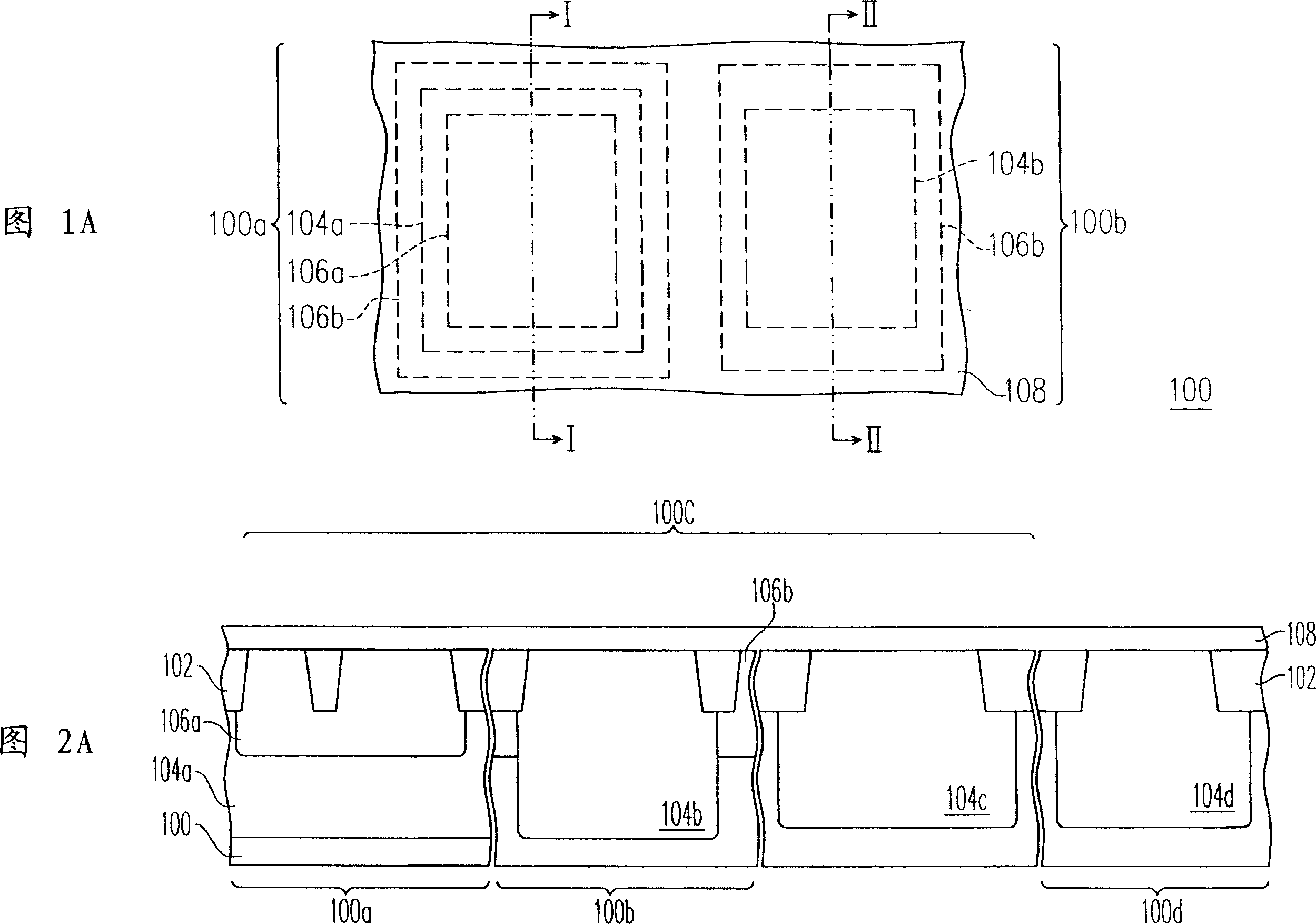
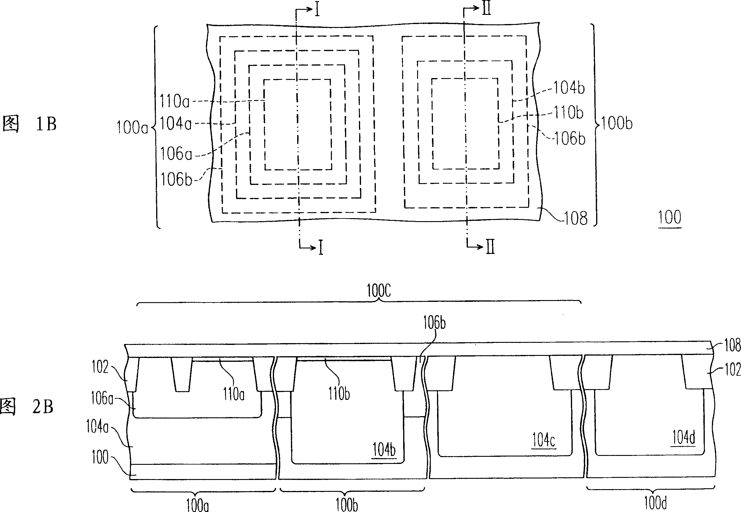
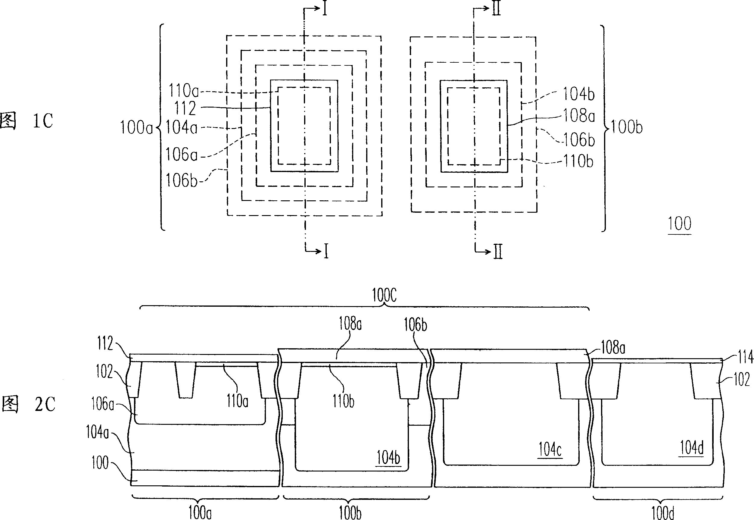
[0061] 1A to FIG. 1D are schematic top views of a method for forming a depleted single-layer polysilicon electrically erasable programmable read-only memory cell according to a preferred embodiment of the present invention. 2A to 2D are schematic cross-sectional views of FIGS. 1A to 1D along line I-I and line II-II, respectively.

[0062] Referring to FIG. 1A and FIG. 2A, a substrate 100 is provided, wherein the substrate 100 has a floating region 100a and a control region 100b. It should be noted that both the floating region 100 a and the control region 100 b are located in a high voltage device region 100 c of the substrate 100 . In addition, the substrate 100 includes a low-voltage device region 100d in addition to the high-voltage device region 100c. Moreover, each device region in the substrate 100 is isolated from each other by an isolation structure 102 . The isolation structure 102 is, for example, a shallow trench isolation structure.

[0063] After that, an isola...


PUM


Abstract

The present invention relates to a method for producing storage cell characterized in depletion type, single layer, polysilicion, electrical erase and programme read only. The method includes the steps as follows: providing a substrate which consists of a floating area and a control area, forming a separated pit area and a pit area respectively in the substrate of the floating area and the control area; next, establishing a well region and a separated well region respectively in the separated pit area and the substrate between the separated pit area and the well region; forming a depletion dope area and a storage cell injecting area respectively in the well area and the pit area; constructing a floating grid which crosses the floating area and the control area on the substrate. Wherein, the floating grid exposes part of the depletion dope area as well as part of the storage cell injecting area; finally, carrying out a technique of doping for the aim of forming a source electrode or drain electrode area and a heavy dope area respectively in the exposed part of the depletion dope area and the storage cell injecting area.

Description

technical field [0001] The present invention relates to a non-volatile memory cell, its forming method and operation method, and in particular to a single-poly EEPROM cell (single-poly EEPROM cell), its manufacturing method and its operation method. Background technique [0002] With the popularity of consumer electronic products, non-volatile memory (non-volatile memory), which can retain stored data and data even when the power is turned off, is widely used in various electronic devices , including multimedia or portable multimedia application devices, such as digital cameras, walkmans, or portable phones. The integration process of non-volatile memory with other devices, such as CMOS, logic device, high voltage device and low voltage device, has become one of the current manufacturing development trends. [0003] The existing Electrically Erasable Programmable Read-Only Memory (EEPROM) is a non-volatile memory. A general EEPROM cell has two stacked gates, including a f...

Claims


Application Information

Patent Timeline
Patent Type & Authority Applications(China)
IPC IPC(8): H01L21/8247H01L21/336
Inventor 陈荣庆董明宗
Owner UNITED MICROELECTRONICS CORP
Why Eureka
Try Eureka