Method for making ceramic electronic part, and plating bath

一种电子部件、制造方法的技术,应用在电容器制造、固定电容的零部件、电气元件等方向,能够解决Sn镀膜表面难包覆、电极可钎焊性下降等问题,达到稳定可钎焊性、可钎焊性改善、膜厚偏差降低的效果

Active Publication Date: 2008-02-20
MURATA MFG CO LTD
View PDF1 Cites 4 Cited by
  • Summary
  • Abstract
  • Description
  • Claims
  • Application Information

AI Technical Summary

Problems solved by technology

[0008] However, when a ceramic electronic component is produced using the Sn plating bath described in Patent Document 1, the solderability of the electrode having the Sn plating film on the outer surface may decrease.
That is, it may be difficult to reliably coat the surface of the Sn plated film with solder

Method used


Image

  • Method for making ceramic electronic part, and plating bath

Examples


Embodiment Construction

[0020] Hereinafter, details of the present invention will be described based on specific embodiments and examples.

[0021] In the method of manufacturing a ceramic electronic component according to the present invention, first, an electronic component formed body composed of a ceramic containing Ba is prepared. Ba-containing ceramics are not particularly limited, but examples thereof include barium titanate-based dielectric ceramics, barium-aluminum-silica-based glass ceramics, and the like.

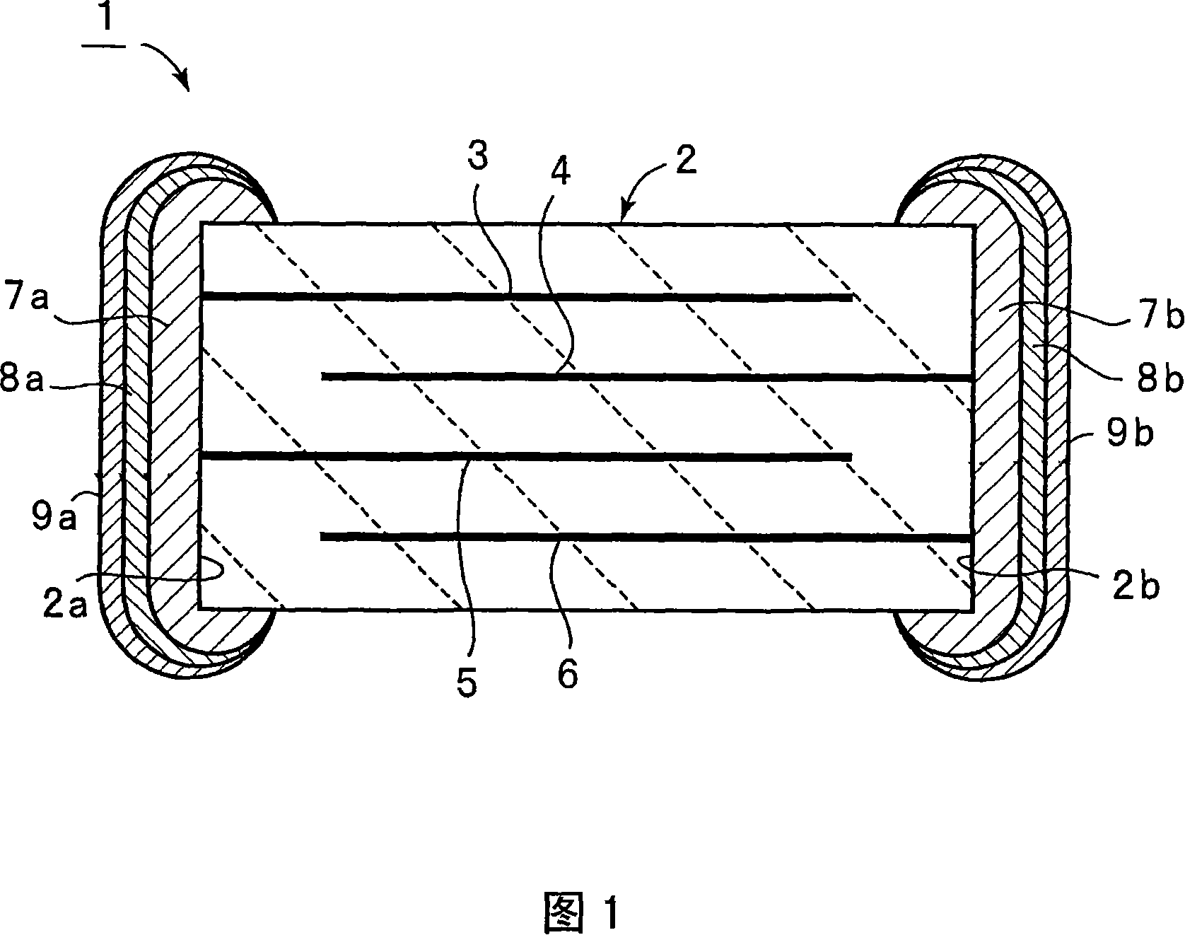
[0022] In addition, the above-mentioned electronic component formed body may be an electronic component formed body composed only of Ba-containing ceramics, or may be a laminated ceramic sintered body in which a plurality of internal electrodes are provided in Ba-containing ceramics.

[0023] In the present invention, after the electronic component forming body is prepared, an electrode having a Sn film is formed on the outer surface of the electronic component forming body. The struct...


PUM

PropertyMeasurementUnit
capacitanceaaaaaaaaaa
current densityaaaaaaaaaa

Abstract

A method for manufacturing a ceramic electronic component, comprising: a step of preparing an electronic component forming body composed of Ba-containing ceramics; and a step of forming an electrode on the outer surface of the electronic component forming body, and the electrode has a The Sn coating film is characterized in that, as the plating bath used when forming the Sn coating film, the Sn ion concentration A is 0.03 to 0.51 mol / L, the sulfate ion concentration B is 0.005 to 0.31 mol / L, and the molar ratio A plating bath with a B / A of less than 1 and a pH in the range of 6.1 to 10.5. According to the present invention, when the Sn plating film is formed, the elution of Ba from the electronic component formed body hardly occurs, not only the adhesion between the electronic component formed bodies caused by the Sn plating film hardly occurs, but also the solderability is good. Method for manufacturing ceramic electronic components.

Description

technical field [0001] The present invention relates to a manufacturing method and a plating bath of ceramic electronic components such as ceramic capacitors, and more particularly relates to a manufacturing method of ceramic electronic components having an Sn plated film in an electrode and an improved formation process of the Sn plated film, and a method for the production thereof. method, etc. of the plating bath. Background technique [0002] Conventionally, in electronic components such as ceramic capacitors, in order to improve the solderability of the external electrodes, Sn plating is often formed on the surface of the external electrodes. When forming a Sn plated film by electroplating, a sulfuric acid bath, a sulfamic acid bath, an alkanesulfonic acid bath, an alkanolsulfonic acid bath, a fluoboric acid bath, or a phenolsulfonic acid bath has conventionally been used. [0003] However, when a sulfamic acid bath or an alkanesulfonic acid bath is used, there is a pr...

Claims


Application Information

Patent Timeline
Patent Type & Authority Applications(China)
IPC IPC(8): C25D3/30C25D7/00
CPCH01G4/1227C25D3/30H01G13/00H01G4/005C25D11/34C25D5/54Y10T29/435Y10T29/43Y10T29/49002Y10T29/42Y10T29/4902C23C18/1653
Inventor 元木章博小川诚松本诚一高野良比古国司多通夫
Owner MURATA MFG CO LTD
Why Eureka
Try Eureka