Multi-chip stacking type packaging structure

A technology of packaging structure and stacking structure, which is applied in the direction of semiconductor/solid-state device parts, semiconductor devices, electrical components, etc., can solve the problems of unable to stack chips, unable to reduce the thickness of stacked packages, and unable to chip

Inactive Publication Date: 2008-02-27
CHIPMOS TECH INC
View PDF0 Cites 9 Cited by
  • Summary
  • Abstract
  • Description
  • Claims
  • Application Information

AI Technical Summary

Problems solved by technology

Obviously, this method of stacking packages with spacers 130 cannot reduce the thickness of the stacked packages, so the number of chips that can be stacked is limited.
[0006] In the stacked package structure in Fig. 1 and Fig. 2, there is also a common problem, that is, the setting position of the spacer 130 cannot give full support to the upper chip (120b; 20), so when performing wire bonding (wire bonding) , if the chip is too thin, it may cause the chip to be broken during the wire bonding process (wafer broken)
Therefore, the chips in the stacked package structure using the spacer 130 need to have a certain thickness, so this stacked package structure cannot stack too many chips.
In addition, in the process of chip stacking, there may also be a problem that the upper chip (120b; 20) contacts the lower wire 140, resulting in a short circuit
In addition, in the stack package structure with the spacer 130, after the wire bonding process is completed, the molding is performed, but since the distance between the upper and lower chips is only the thickness of the spacer 130 or the spacer layer 50 , so it may form a void in the gap between the upper and lower chips. When the bubble is expanded by high temperature, it will cause cracks in the encapsulant

Method used


Image

  • Multi-chip stacking type packaging structure
  • Multi-chip stacking type packaging structure
  • Multi-chip stacking type packaging structure

Examples


Embodiment Construction

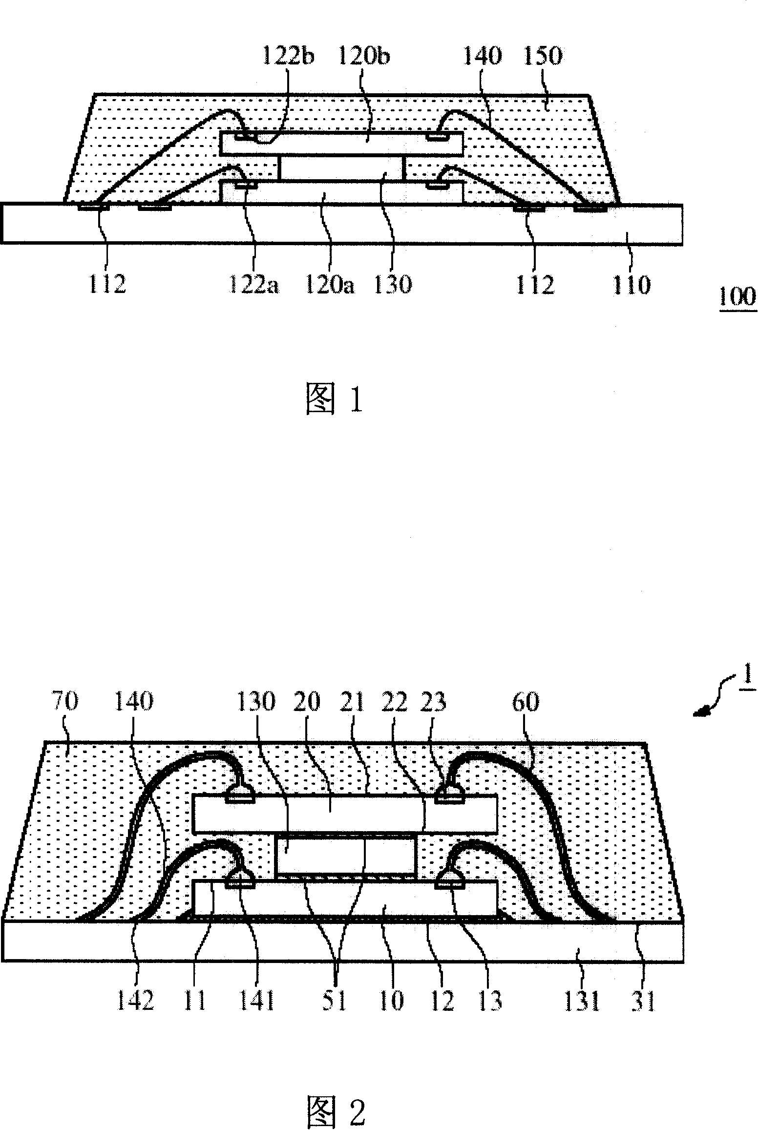
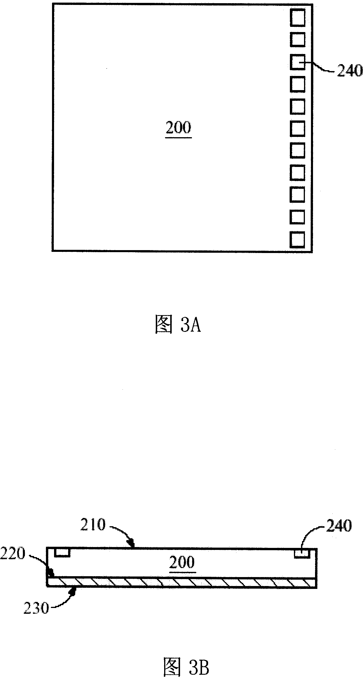
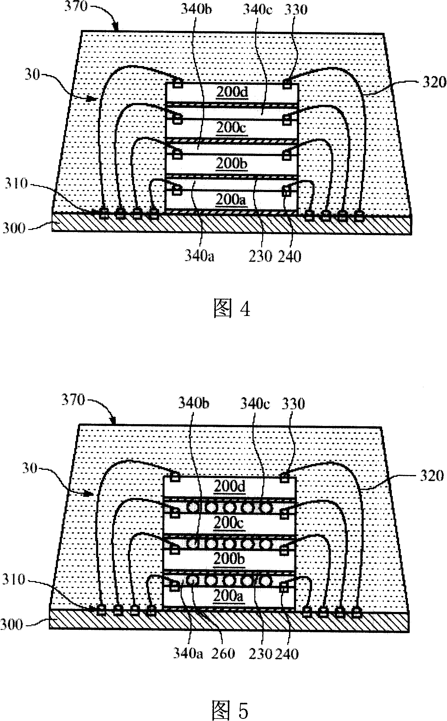
[0061] The direction discussed in the present invention is a way of using multi-chip stacking to stack multiple chips with similar sizes into a three-dimensional packaging structure. In order to provide a thorough understanding of the present invention, detailed packaging structures and packaging steps will be presented in the following description. Obviously, the practice of the present invention is not limited to the specific details of the manner in which chips are stacked that are familiar to those skilled in the art. On the other hand, well-known chip formation methods and detailed steps of back-end processes such as chip thinning are not described in detail to avoid unnecessary limitations of the present invention. However, for the preferred embodiments of the present invention, it will be described in detail as follows, but in addition to these detailed descriptions, the present invention can also be widely implemented in other embodiments, and the scope of the present ...


PUM


Abstract

The present invention provides a multi-chip-stacked package, and includes: a substrate set with several metal terminals and a multi-chip-stacked package are provided; the multi-chip-stacked package is fixed on substrate, of which active surface of each chip is set with several welding pads, and each chip is set with insulating layer on its back; a clinging layer combines the active surface of each chip and the insulating layer set on the back of the other chip to form stack structure; several metal wires joins the several welding pads on the several chips and the several metal terminals on the substrate.

Description

technical field [0001] The present invention relates to a multi-chip stacking package structure, and in particular to a multi-chip stacking structure in which a reverse lead bonding process and an insulating layer are used to reduce the arc of metal wires, and the adhesive layer of the multi-chip stacking structure is added with Approximate spherical packaging structure. Background technique [0002] In recent years, three-dimensional (3D) packaging is being carried out in the back-end process of semiconductors, in order to use the least area to achieve relatively large semiconductor integration (Integrated) or memory capacity. In order to achieve this goal, a method of using chip stacked (chip stacked) to achieve three-dimensional space (Three Dimension; 3D) packaging has been developed at this stage. [0003] In the known technology, the chip stacking method is to stack multiple chips on the substrate, and then use a wire bonding process to connect the multiple chips to t...

Claims


Application Information

Patent Timeline
Patent Type & Authority Applications(China)
IPC IPC(8): H01L25/00H01L23/49
CPCH01L2224/32145H01L2224/48465H01L2224/73265H01L2224/32245H01L2224/48247H01L2224/48227H01L2224/32225H01L2924/181H01L2924/00H01L2924/00012
Inventor 林鸿村
Owner CHIPMOS TECH INC
Why Eureka
Try Eureka