Wafer testing module

A chip testing and chip technology, which is applied in the field of semiconductor testing equipment, can solve the problems of increasing failure rate, shutting down or restarting, and increasing the burden of online testers, etc., and achieves the effect of low production cost and thin and light appearance

Inactive Publication Date: 2008-03-05
ADVANCED SEMICON ENG INC
View PDF0 Cites 7 Cited by
  • Summary
  • Abstract
  • Description
  • Claims
  • Application Information

AI Technical Summary

Problems solved by technology

[0005] However, since the automatic test equipment interface components are quite large and expensive, the known chip test modules often cause problems in terms of space utilization and cost considerations.
Especially in equipment maintenance, the failure rate will increase due to the complicated assembly of mechanical components. Once a failure occurs or the electrical test fails, the entire test system will stop or restart, thus increasing the burden on online testers

Method used


Image

  • Wafer testing module
  • Wafer testing module
  • Wafer testing module

Examples


Embodiment Construction

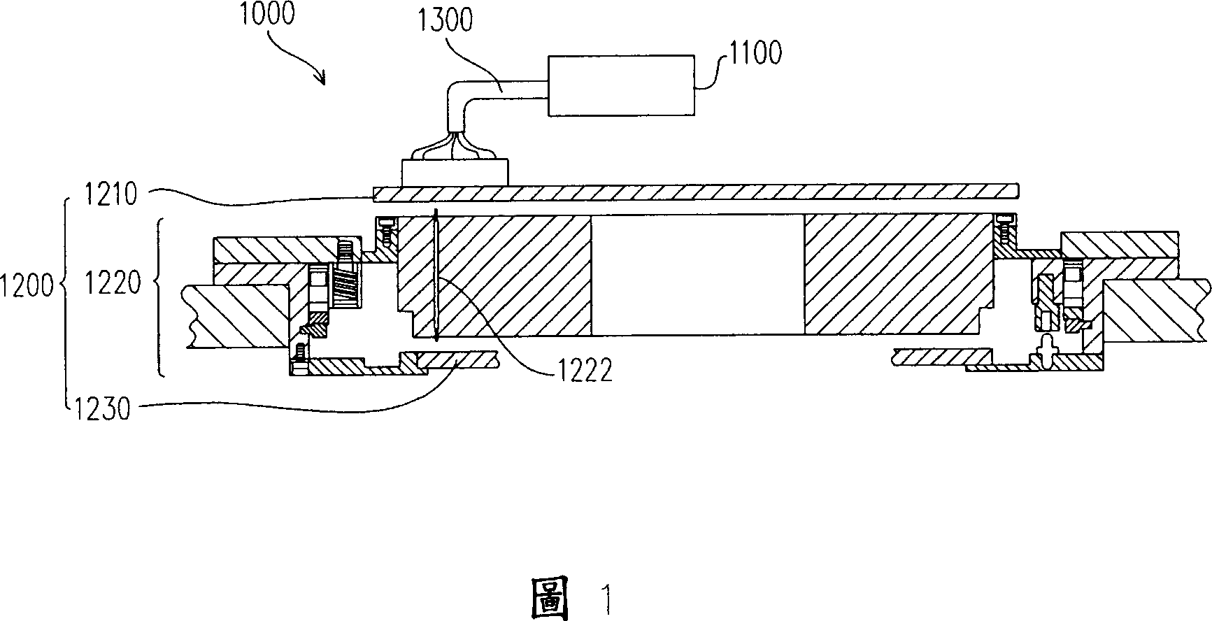
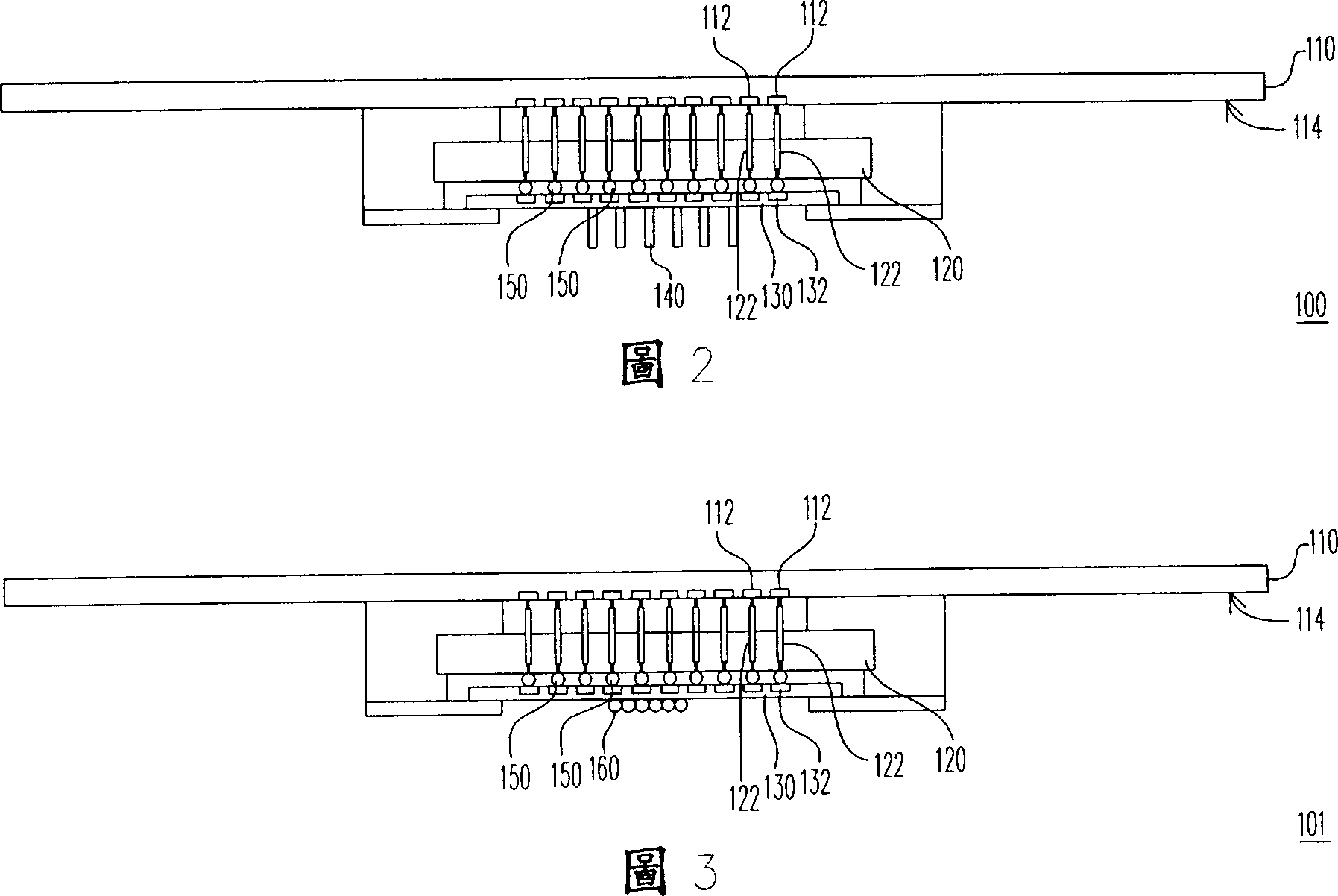
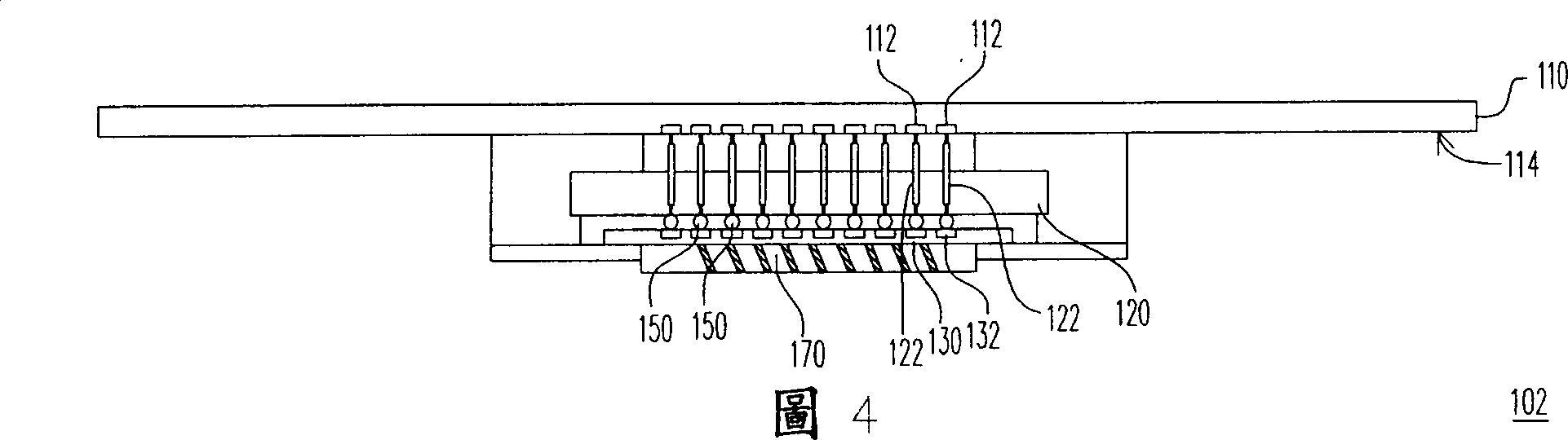
[0048] FIG. 2 is a schematic diagram of a wafer testing module according to an embodiment of the present invention. Referring to FIG. 2 , the chip test module 100 mainly includes a test load board 110 , a pod socket 120 , a substrate 130 and a plurality of probes 140 . The test load board 110 has a plurality of first contacts 112 , wherein the first contacts 112 are located on a surface 114 of the test load board 110 . The test load board 110 is, for example, a printed circuit board (PCB) or a circuit board manufactured by other types of processes, and its function is similar to the circuit board 1210 for electrically transmitting test signals of the chip test system 1100 in FIG. 1 . It is worth noting that the pogo pin socket 120 is configured on the test load board 110, and the pogo pin socket 120 is provided with a plurality of retractable pogo pins 122, which are used to replace the probe contact seat and complex Unique positioning mechanism and lifting self-locking mecha...


PUM


Abstract

The invention comprises: a test load-bearing board, a jack of spring contact pin, a baseboard and multi probes. The test load-bearing board has multi first contact points; said jack of spring contact pin is located at the test load-bearing board, there are multi spring contact pins in the jack of spring contact pin; the baseboard is secured on the jack of spring contact pin and has multi second contact points; said spring contact pins are respectively used to connect each first contact point to the second contact point; said multi probes are located on the baseboard and are used for electrically connecting to a wafer.

Description

【Technical field】 [0001] The present invention relates to a semiconductor testing device, and in particular to a wafer testing device. 【Background technique】 [0002] In the manufacturing process of integrated circuits or chips, no matter at which stage of the process, it is necessary to perform electrical tests on integrated circuits or chips. Every integrated circuit, no matter in wafer form or packaged form, must be tested to determine whether it is a good product and to determine its electrical characteristics. As the output of integrated circuits continues to increase, the functions of integrated circuits are becoming more powerful, and their structures are becoming more and more complex, so the demand for high-speed and accurate testing is more urgent. [0003] The process of individually testing integrated circuits on a wafer before they have been diced into individual dies is called wafer probing. During the wafer probing process, automatic test equipment (ATE) est...

Claims


Application Information

Patent Timeline
Patent Type & Authority Applications(China)
IPC IPC(8): G01R31/00G01R31/26G01R31/28H01L21/66
Inventor 黄贵麟吕智弘全清成
Owner ADVANCED SEMICON ENG INC
Why Eureka
Try Eureka