Supercharge Your Innovation With Domain-Expert AI Agents!

Flash memory device

A technique of etching and stacking gates, which is applied in the field of manufacturing flash memory devices, and can solve problems such as reduced realizability and poor efficiency of flash memory devices

Inactive Publication Date: 2008-03-12
DONGBU HITEK CO LTD
View PDF1 Cites 2 Cited by
  • Summary
  • Abstract
  • Description
  • Claims
  • Application Information

AI Technical Summary

Problems solved by technology

Also, even if a photoresist pattern can be formed, it reduces its realizability and degrades the efficiency of the flash memory device

Method used


Image

  • Flash memory device
  • Flash memory device
  • Flash memory device

Examples


Embodiment Construction

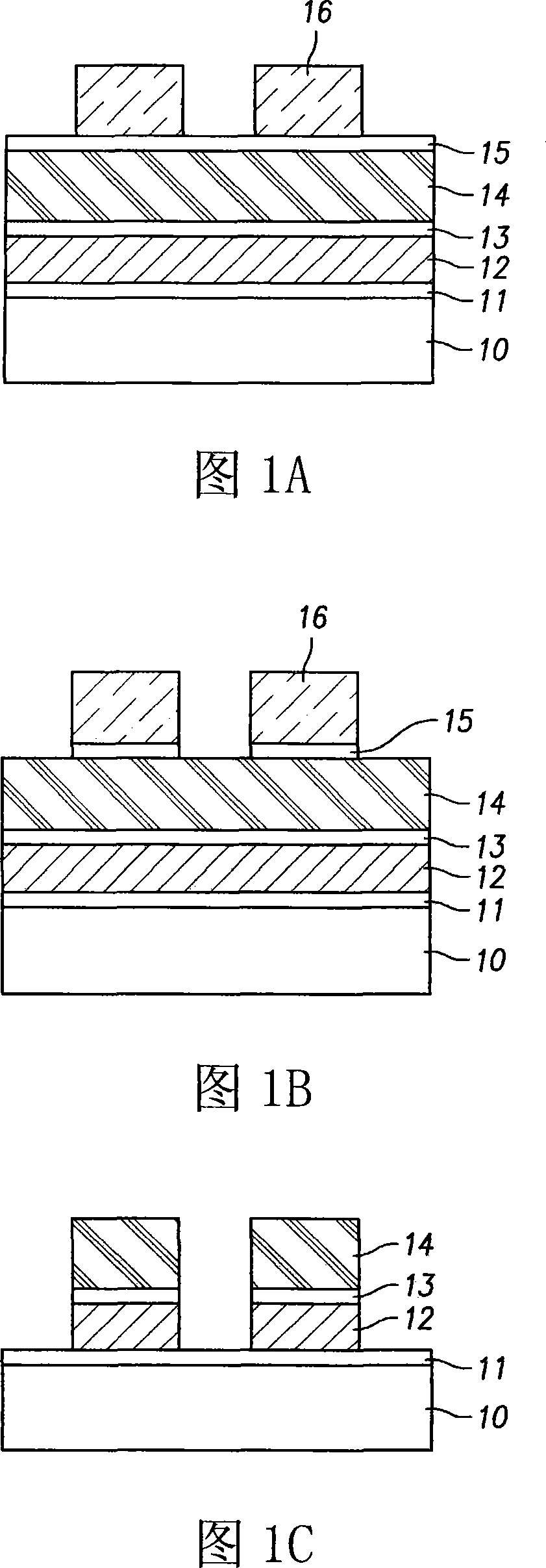
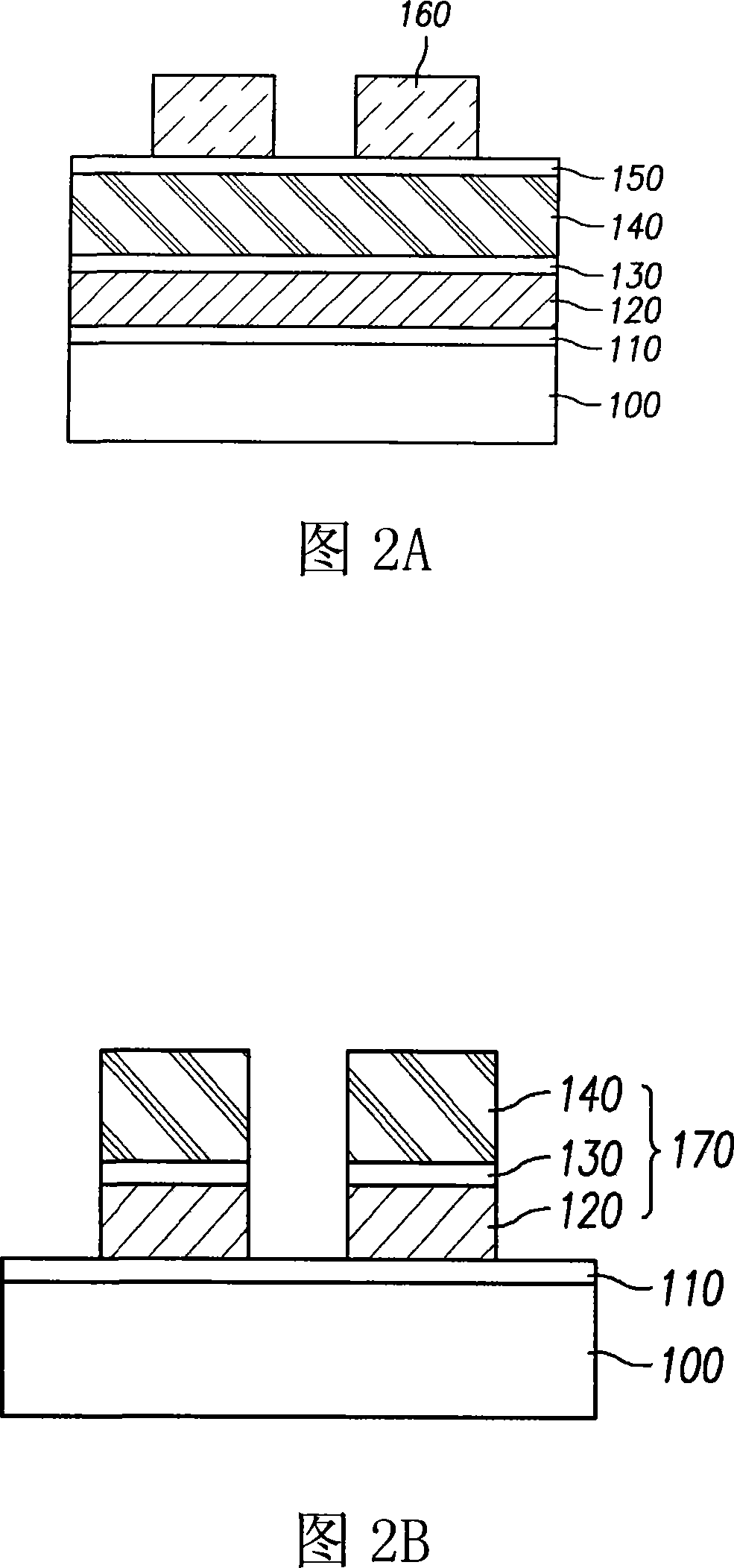
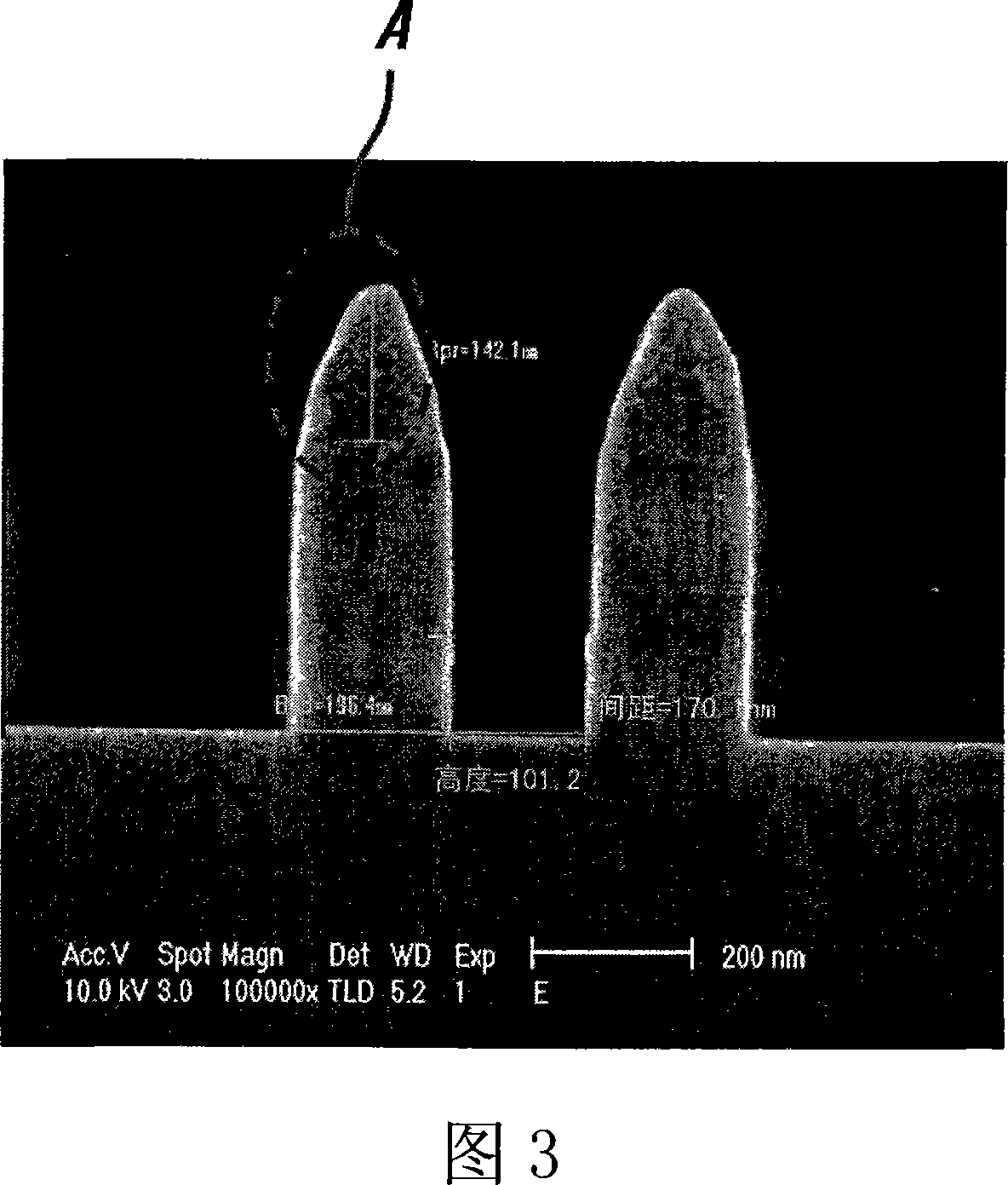
[0016] Referring to FIG. 2A, an oxide film 110, a floating gate polysilicon film 120, an oxide-nitride-oxide (ONO) film 130, a control gate polysilicon film 140, and a bottom anti-reflective film are sequentially stacked on a semiconductor substrate 100. Coating (BARC) 150. To form the stacked gate, a photoresist for KrF is coated with a thickness between approximately 4000 Ȧ and 5000 Ȧ.

[0017] The photoresist for KrF is patterned to form a photoresist pattern 160 for KrF. After obtaining a depth of focus (DOF) margin in the exposure process, the BARC 150 and the stacked gate film including the floating gate polysilicon film 120, the ONO film 130, and the control gate polysilicon film 140 are etched together. . According to an embodiment, the etching method is different from the related art etching method which first etches the BARC 15 using the photoresist pattern 16 (as shown in FIG. 1B ), and then etches the floating gate polysilicon film 12, the ONO film 13 and Contro...


PUM


Abstract

Embodiments relate to a flash memory device and a method of manufacturing a flash memory device that may improve a reliability of process by obtaining a Depth of Focus (DOF) in an exposure process. In embodiments, a method may include sequentially stacking an oxide film, a floating gate poly film, an ONO film, a control gate poly film, and a BARC (Bottom AntiReflect Coating) on a semiconductor substrate, forming a photoresist pattern for a stack gate on the BARC, and etching the BARC, the control gate poly film, the ONO film and the floating gate poly film at once by using the photoresist pattern until the oxide film is exposed.

Description

[0001] This application claims priority from Korean Patent Application No. 10-2006-0085485 filed on September 6, 2006, which is hereby incorporated by reference. technical field [0002] The invention relates to a manufacturing method of a flash memory device, in particular to a manufacturing method of a flash memory device that improves process reliability by obtaining a depth of focus (DOF) in an exposure process. Background technique [0003] The gate coupling coefficient is an important factor in determining the efficiency of a memory cell in a flash memory device. The gate coupling coefficient has a significant effect on the potential of the floating gate. The potential of the floating gate in a flash memory device having a higher gate coupling coefficient is close to a given potential of a control gate in a memory cell. Therefore, the performance of the flash memory cell, including program and erase efficiency and fast read speed, can be improved. [0004] A high gat...

Claims


Application Information

Patent Timeline
IPC IPC(8): H01L21/28H01L21/336H01L29/788
CPCH01L21/31138H01L27/11521H01L29/42324H01L21/32137H01L21/28273H01L27/115H01L21/31116H01L29/40114H10B69/00H10B41/30
Inventor 张郑烈
Owner DONGBU HITEK CO LTD
Features
  • R&D
  • Intellectual Property
  • Life Sciences
  • Materials
  • Tech Scout
  • Unparalleled Data Quality
  • Higher Quality Content
  • 60% Fewer Hallucinations
Learn More