
Displacement cache, grid drive circuit and liquid crystal display possessing frame doubling frequency

A technology of shift register and shift register unit, which is applied in the field of shift register and gate drive circuit, which can solve the problems of high cost and reduce the yield rate of liquid crystal display, and achieve the effect of reducing the number

Active Publication Date: 2008-03-19
AU OPTRONICS CORP
View PDF0 Cites 4 Cited by
  • Summary
  • Abstract
  • Description
  • Claims
  • Application Information

AI Technical Summary

Problems solved by technology

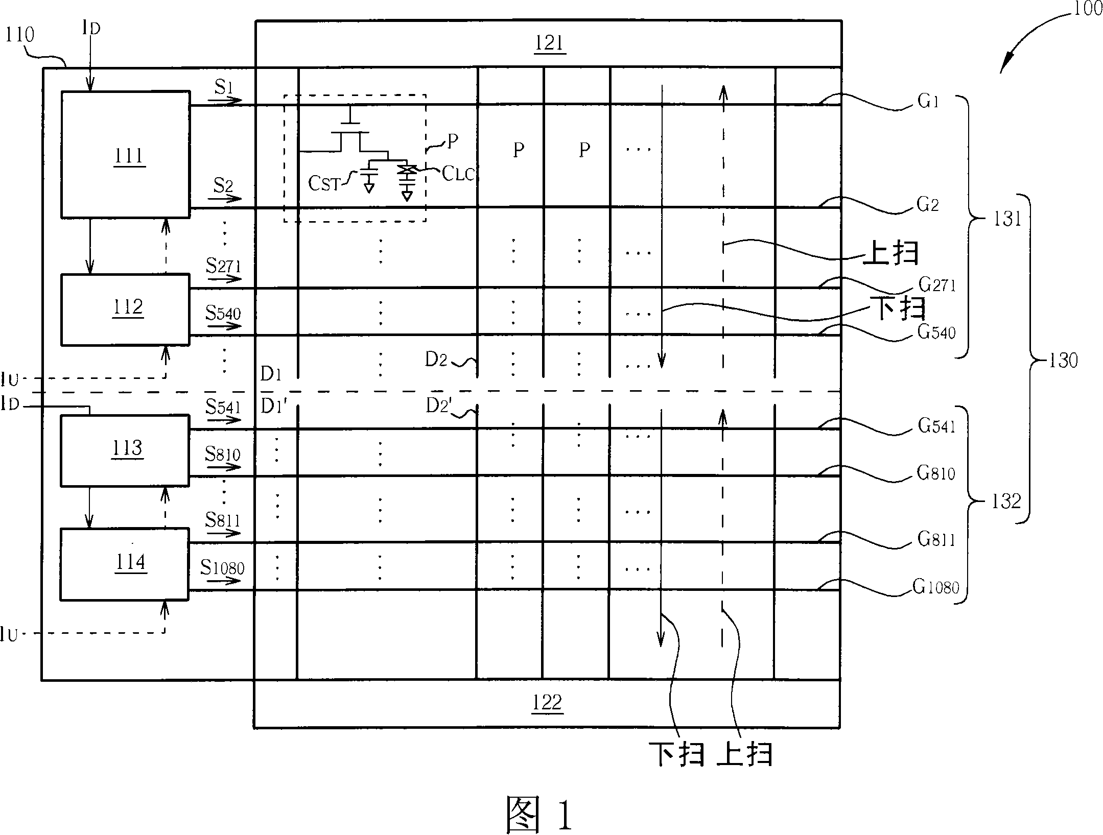
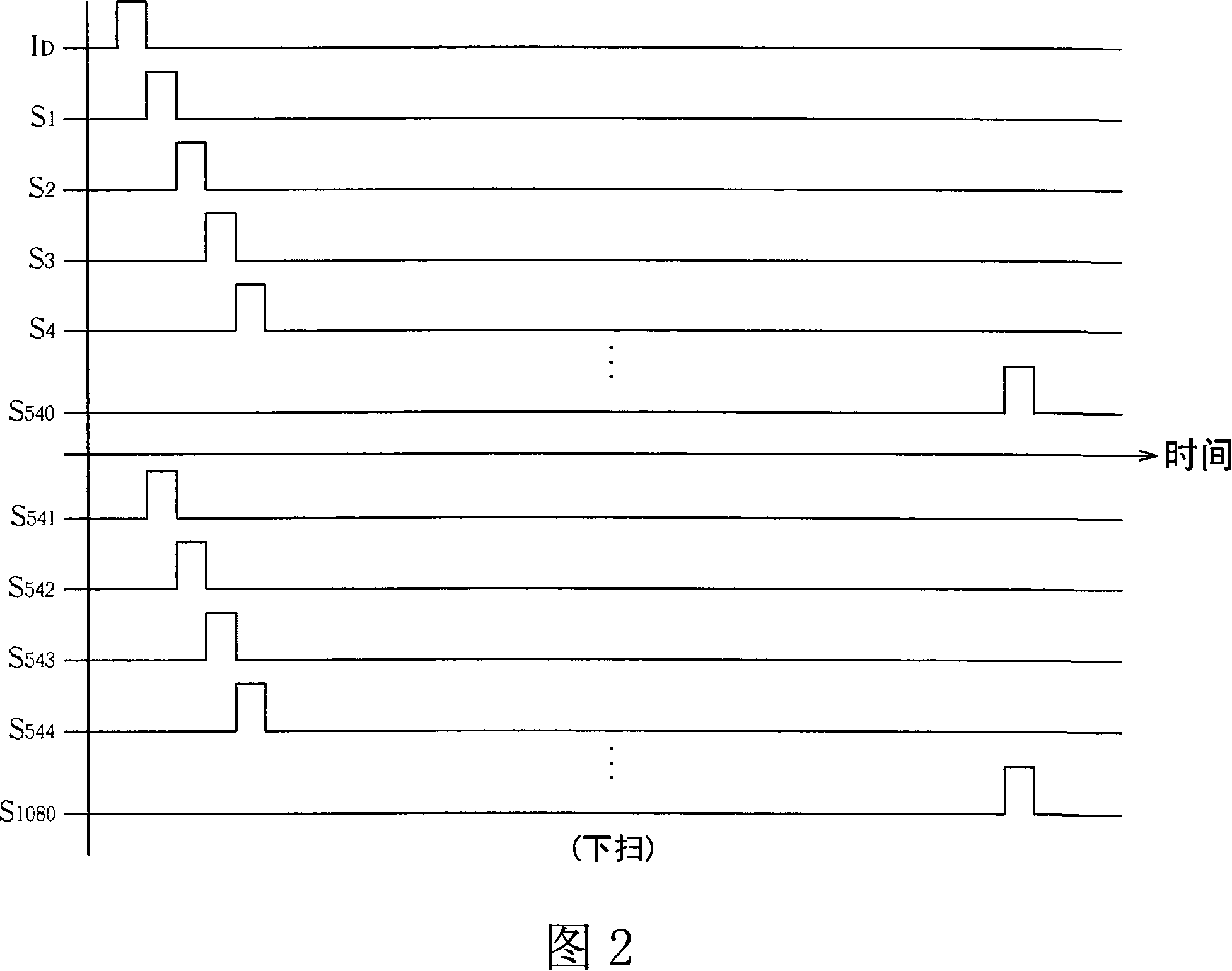
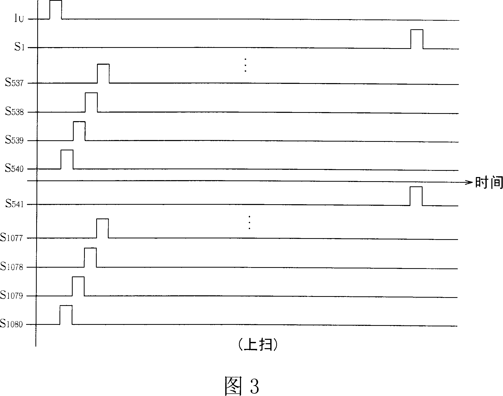
[0005] Therefore, the two regions such as the upper display region 131 and the lower display region 132 can pass through the gate drivers 111, 112 and 113, 114 respectively belonging to the two regions within a frame frequency of 120 Hz, and sequentially (from top to bottom or from bottom to bottom) scanning in the upward direction) to generate gate drive signals to drive the liquid crystal display; but the disadvantage of the above architecture is that the number of single-side gate drivers needs to be 2N (wherein N is a positive integer, and N is the upper display area or the lower display area) The number of gate drivers on both sides of the display area), and a larger total number of drivers will not only reduce the yield of the LCD display, but also require higher costs

Method used


Image

  • Displacement cache, grid drive circuit and liquid crystal display possessing frame doubling frequency
  • Displacement cache, grid drive circuit and liquid crystal display possessing frame doubling frequency
  • Displacement cache, grid drive circuit and liquid crystal display possessing frame doubling frequency

Examples


Embodiment Construction

[0040] Please refer to Figure 4. FIG. 4 is a schematic diagram of a liquid crystal display with doubled frame frequency according to the present invention. As shown in the figure, the liquid crystal display 400 includes a shift register driving circuit 410 , a signal selection circuit 440 , a voltage shifting circuit 450 , data driving circuits 421 and 422 and a display area 430 . As shown in the figure, the shift register driving circuit 410 , the signal selecting circuit 440 and the voltage shifting circuit 450 form a bidirectional gate driving circuit 460 . The display area 430 includes an upper display area 431 and a lower display area 432 . The data driving circuit 421 is located at the upper end of the display area 430, and is used to transmit corresponding data to the upper display area 431 via the data lines D1, D2...; the data driving circuit 422 is located at the lower end of the display area 430, via the data lines D1', D2' . . . is used to transmit corresponding ...


PUM


Abstract

The invention discloses a shift buffer, a grid drive circuit with two-way transmission and a LCD with double frame frequency. The LCD comprises an upper display zone with c grid lines, a lower display zone with d grid lines and a grid drive circuit, wherein the grid drive circuit comprises a first shift buffer coupled correspondingly with x grid lines in the upper display zone to provide a corresponding grid driving signal, a second shift buffer coupled correspondingly with y grid lines in the lower display zone to provide the corresponding grid driving signal, and a third shift buffer coupled correspondingly with (c-x) grid lines in the upper display zone and (d-y) grid lines in the lower display zone, to provide the corresponding grid driving signal, wherein c, d, x and y are independently an positive integer more than 1, and x is more than 1 but less than c and y is more than 1 but less than d.

Description

technical field [0001] The present invention relates to a shift register and a gate drive circuit formed by the shift register; more specifically, the present invention relates to a liquid crystal display utilizing the frame frequency multiplication of the shift register. Background technique [0002] Please refer to Figure 1. FIG. 1 is a schematic diagram of a traditional double frame rate (double frame rate, 120 Hz) liquid crystal display. As shown in the figure, the liquid crystal display 100 includes a gate driving circuit 110 , two data driving circuits 121 , 122 and a display area 130 . The display area 130 includes an upper display area 131 and a lower display area 132 . The data driving circuit 121 is located at the upper end of the display area 130, and transmits corresponding data to the upper display area 131 via the data lines D1, D2... '..., transmit the corresponding data to the lower display area 132 . Both the upper display area 131 and the lower display ...

Claims


Application Information

Patent Timeline
Patent Type & Authority Applications(China)
IPC IPC(8): G11C19/00H03K19/0175G09G3/36
Inventor 杜明鸿杨智翔
Owner AU OPTRONICS CORP
Learn More