Wafer thinning method

A technology of wafers and polymer materials, applied in electrical components, semiconductor/solid-state device manufacturing, circuits, etc., can solve the problems of stress fragments and warpage, expensive, pollution, etc., and achieve the effect of preventing warpage

Active Publication Date: 2008-03-26
ADVANCED SEMICON ENG INC
View PDF0 Cites 14 Cited by
  • Summary
  • Abstract
  • Description
  • Claims
  • Application Information

AI Technical Summary

Problems solved by technology

[0002] In order to thin the semiconductor package, a grinding process is usually performed on the back of the wafer to thin the wafer, but since the active surface of the wafer has a circuit pattern or is provided with various protruding components, such as bumps or passive components Therefore, when grinding and thinning the backside of the wafer, an adhesive tape or film must be used to protect the active surface and the protruding elements. As shown in Figures 1 and 2, an existing wafer 100 has an active surface 110 and a back surface 120 And a side surface 130 between the active surface 110 and the back surface 120, a plurality of protruding elements 140 are arranged on the active surface 110, an adhesive film 10 covers the active surface 110 of the wafer 100, and the wafer is ground 100, it is used to protect the active surface 110 and these protruding elements 140, but the existing adhesive film 10 is composed of a base layer 11, a super soft layer 12 and an adhesive layer 13, which is expensive and when these protruding elements If the distance between 140 is too small, the adhesive film 10 cannot completely cover the active surface 110 of the wafer 100 and cover the protruding elements 140, so when the back surface 120 of the wafer 100 is ground, the stress generated will easily lead to fracture. and warping
In addition, since the adhesive film 10 does not cover the side 130 of the wafer 100, the wafer 100 will be cracked during grinding, or, when the adhesive film 10 is torn off, the adhesive film 10 will be placed on the active surface. The protruding elements 140 on the surface 110 are peeled off. In addition, if the adhesive film 10 is not removed, there will be residual glue remaining on the active surface 110 to cause pollution.

Method used


Image

  • Wafer thinning method
  • Wafer thinning method
  • Wafer thinning method

Examples


Embodiment Construction

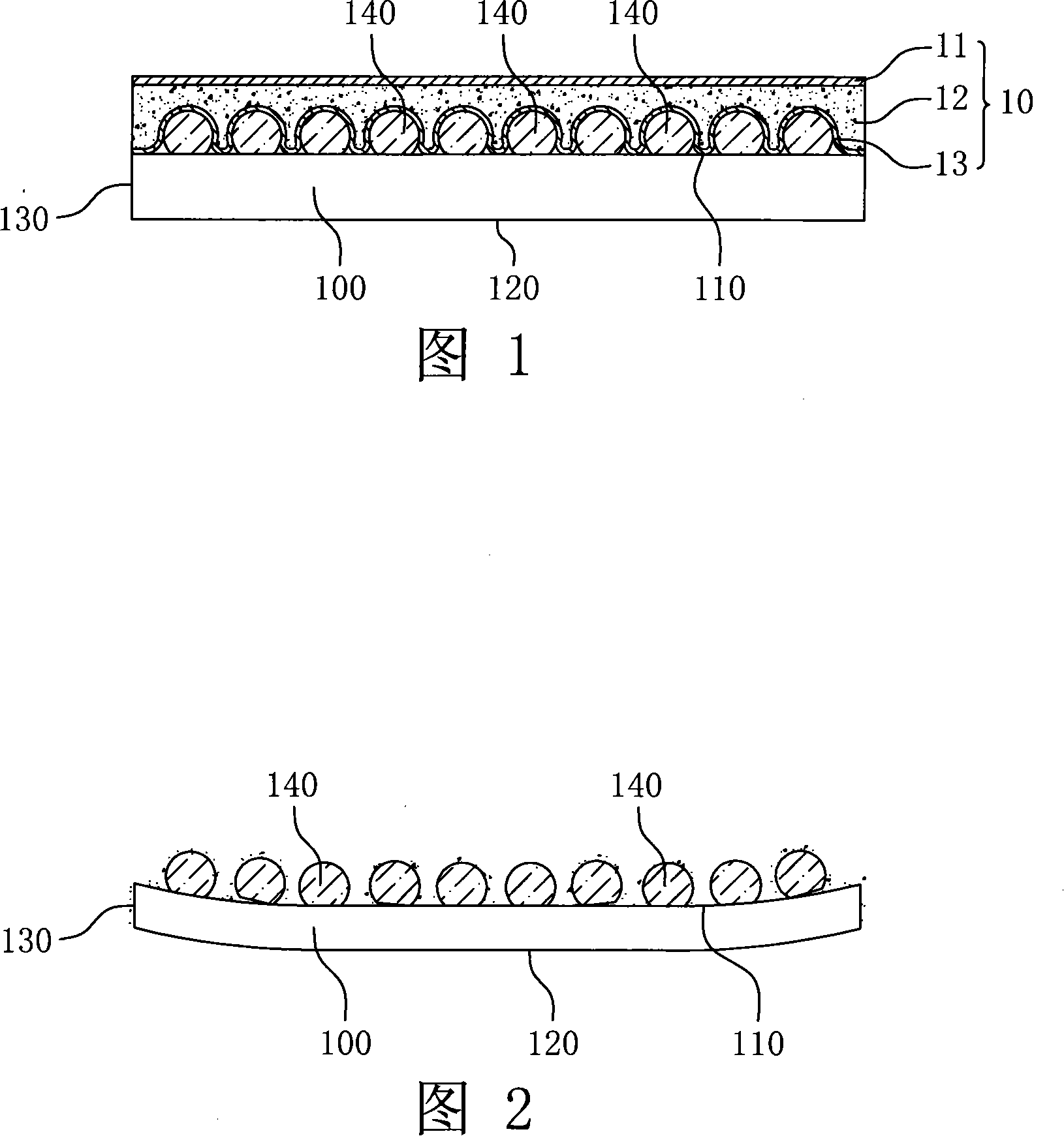
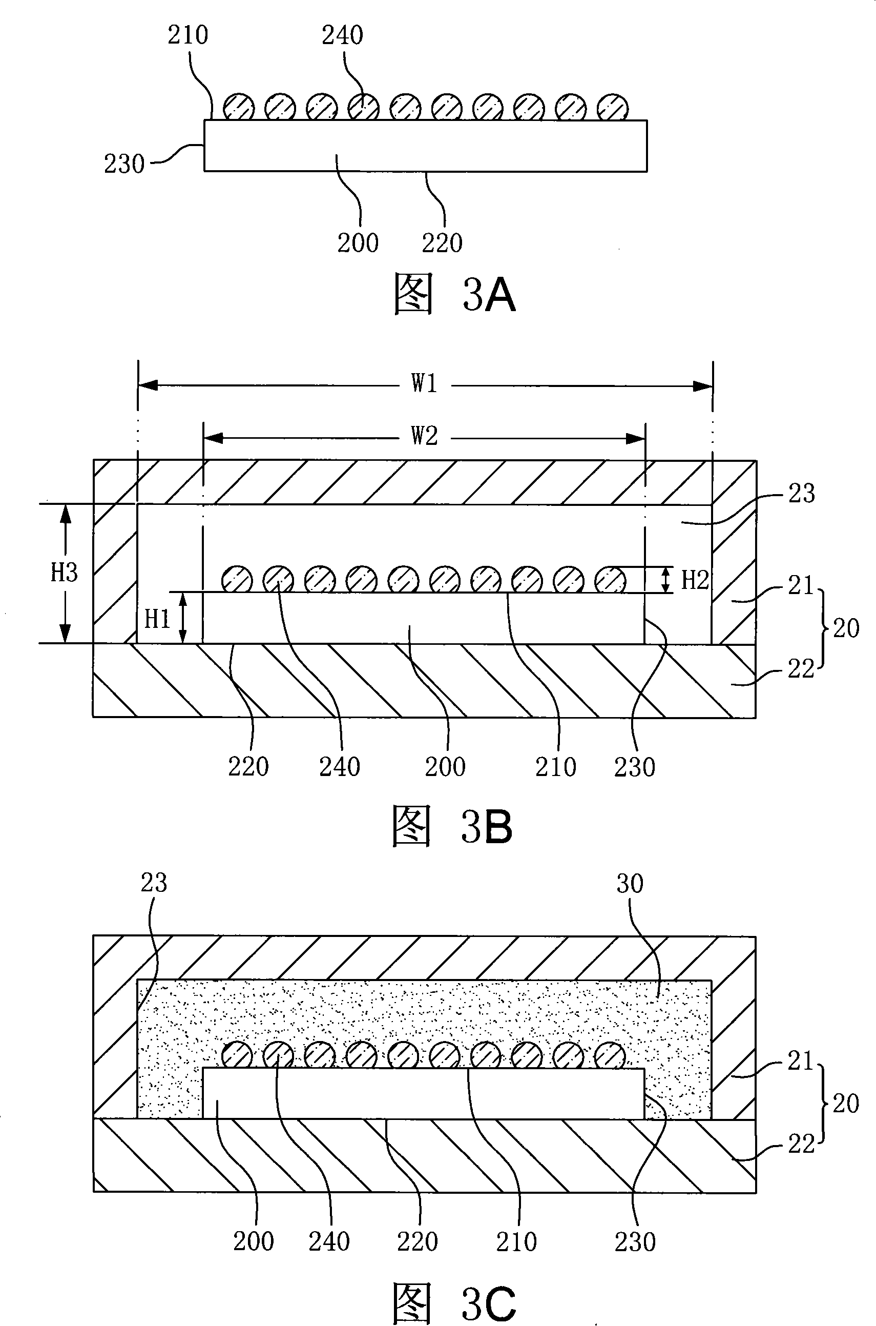
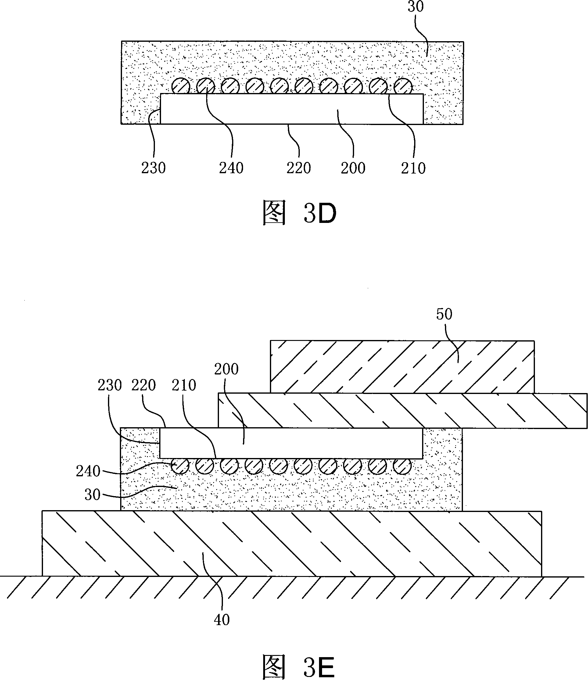
[0016] Please refer to FIG. 3A to FIG. 3E , a wafer thinning method is disclosed according to a first embodiment of the present invention. First, please refer to FIG. 3A , a wafer 200 is provided, and the wafer 200 has an active surface 210 , a rear surface 220 and at least one side surface 230 between the active surface 210 and the rear surface 220. In this embodiment, the active surface 210 of the wafer 200 is provided with several protruding elements 240, and these protruding elements 240 are selected From bumps, solder balls or passive components, in this embodiment, these protruding elements 240 are bumps. Then, referring to FIG. 3B, the wafer 200 is placed in a mold 20. The mold 20 includes an upper mold 21 and a lower mold 22. The upper mold 21 and the lower mold 22 form a mold cavity 23. The wafer 200 is placed On the lower mold 22 , the active surface 210 of the wafer 200 faces the upper mold 21 . In this embodiment, the width W1 of the mold cavity 23 is slightly lar...


PUM


Abstract

This invention relates to a method for getting wafers thinner including: providing a wafer with an active side and a back, setting several hump elements on the active side and putting the wafer in a die and forming a macromolecular material in the die to cover the active side of the wafer at least, solidifying the macromolecular material and removing the die, grinding the back of the wafer to get the wafer thinner, finally, removing the material to expose the active side of the wafer and the hump elements on it, which utilizes the die to enable the macromolecular material to cover the active side of the wafer and wrap the hump elements, in this way, stress generated in grinding the wafer is distributed on the wafer uniformly so as to avoid warp, break, crack of the wafer or peel off of the hump elements.

Description

【Technical field】 [0001] The invention relates to a wafer thinning method, in particular to a wafer thinning method capable of preventing wafer or bumps on the wafer from being damaged. 【Background technique】 [0002] In order to thin the semiconductor package, a grinding process is usually performed on the back of the wafer to thin the wafer, but since the active surface of the wafer has a circuit pattern or is provided with various protruding components, such as bumps or passive components Therefore, when grinding and thinning the backside of the wafer, an adhesive tape or film must be used to protect the active surface and the protruding elements. As shown in Figures 1 and 2, an existing wafer 100 has an active surface 110 and a back surface 120 And a side surface 130 between the active surface 110 and the back surface 120, a plurality of protruding elements 140 are arranged on the active surface 110, an adhesive film 10 covers the active surface 110 of the wafer 100, and...

Claims


Application Information

Patent Timeline
Patent Type & Authority Applications(China)
IPC IPC(8): H01L21/304
Inventor 蔡裕斌黄正一
Owner ADVANCED SEMICON ENG INC
Why Eureka
Try Eureka