

A graphic OSD controller integrated into video processing chip
A video processing and controller technology, applied in the field of graphic OSD controllers, can solve the problems of large storage space and system resources, occupation, complexity increase, etc., and achieve the requirements of saving storage resources, simple structure design, and reducing storage space requirements. Effect
- Summary
- Abstract
- Description
- Claims
- Application Information
AI Technical Summary
Problems solved by technology
Method used
Image

Examples
Embodiment Construction
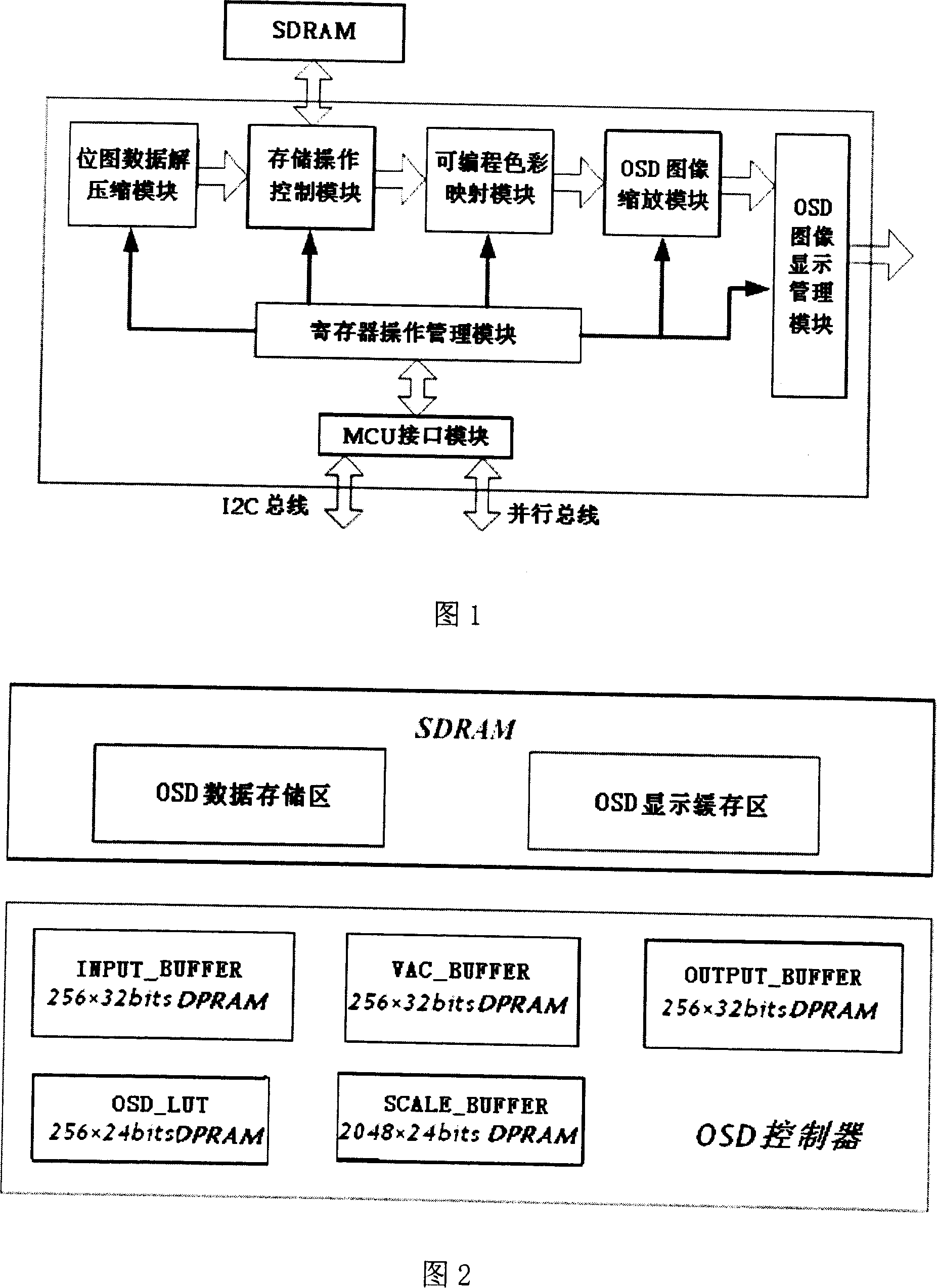
[0038] Referring to Fig. 1, the graphic OSD controller integrated in video processing chip of the present invention, its internal basic structure comprises bitmap data decompression module, storage operation control module, programmable color mapping module, OSD image scaling module, OSD image display management Module, register operation management module and MCU interface module; the user sets the registers and control parameter output of the register operation control module through the MCU interface, so as to complete various functions such as storage operation, color mapping and display synthesis.
[0039] After the bitmap data is compressed, the storage space requirement for off-chip bitmap data can be effectively reduced. The bitmap data decompression module is used to decompress OSD data into bitmap index data. The data compression adopts the improved run-length encoding (BLE) algorithm, and the compression part is realized by software.
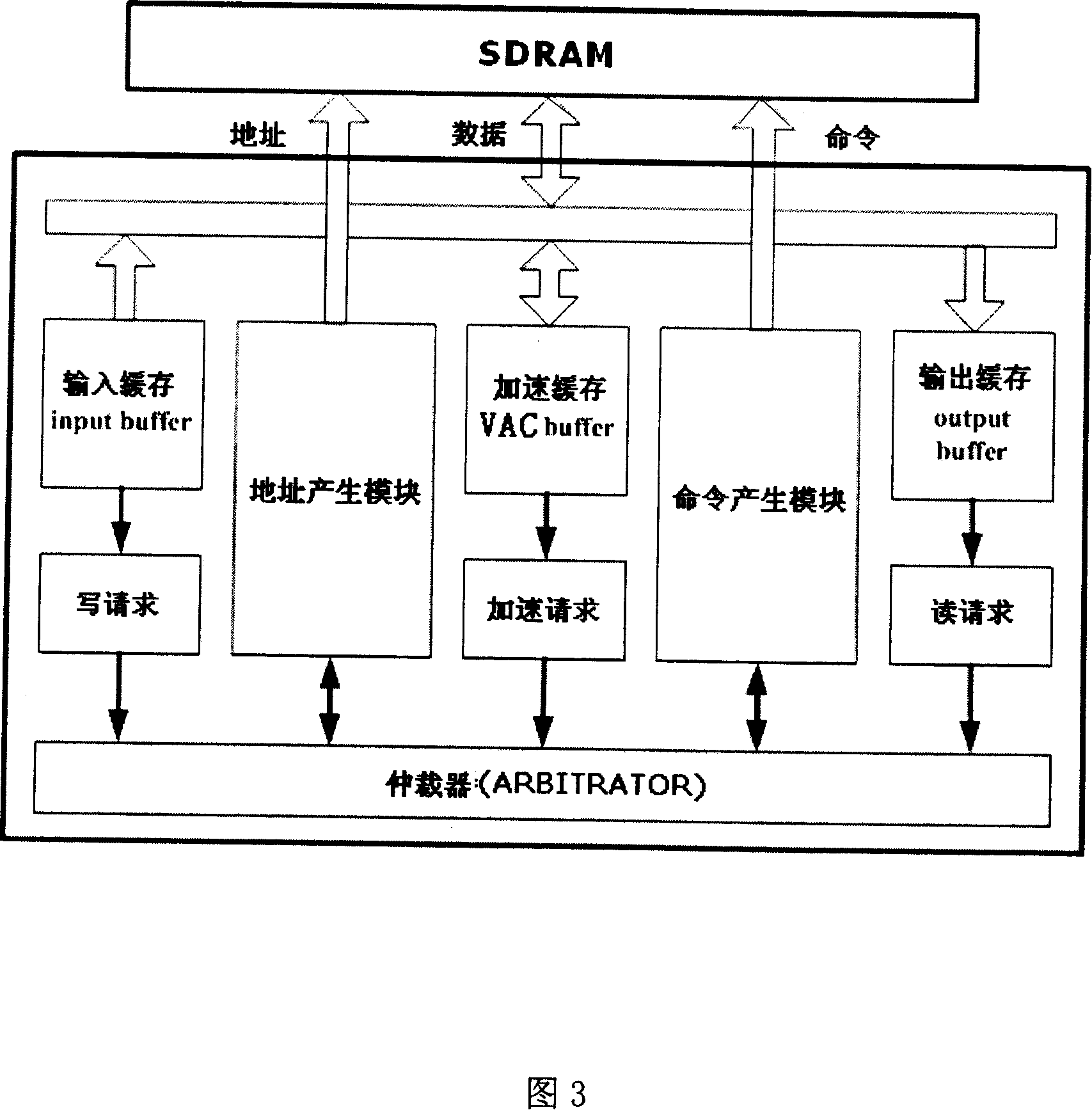
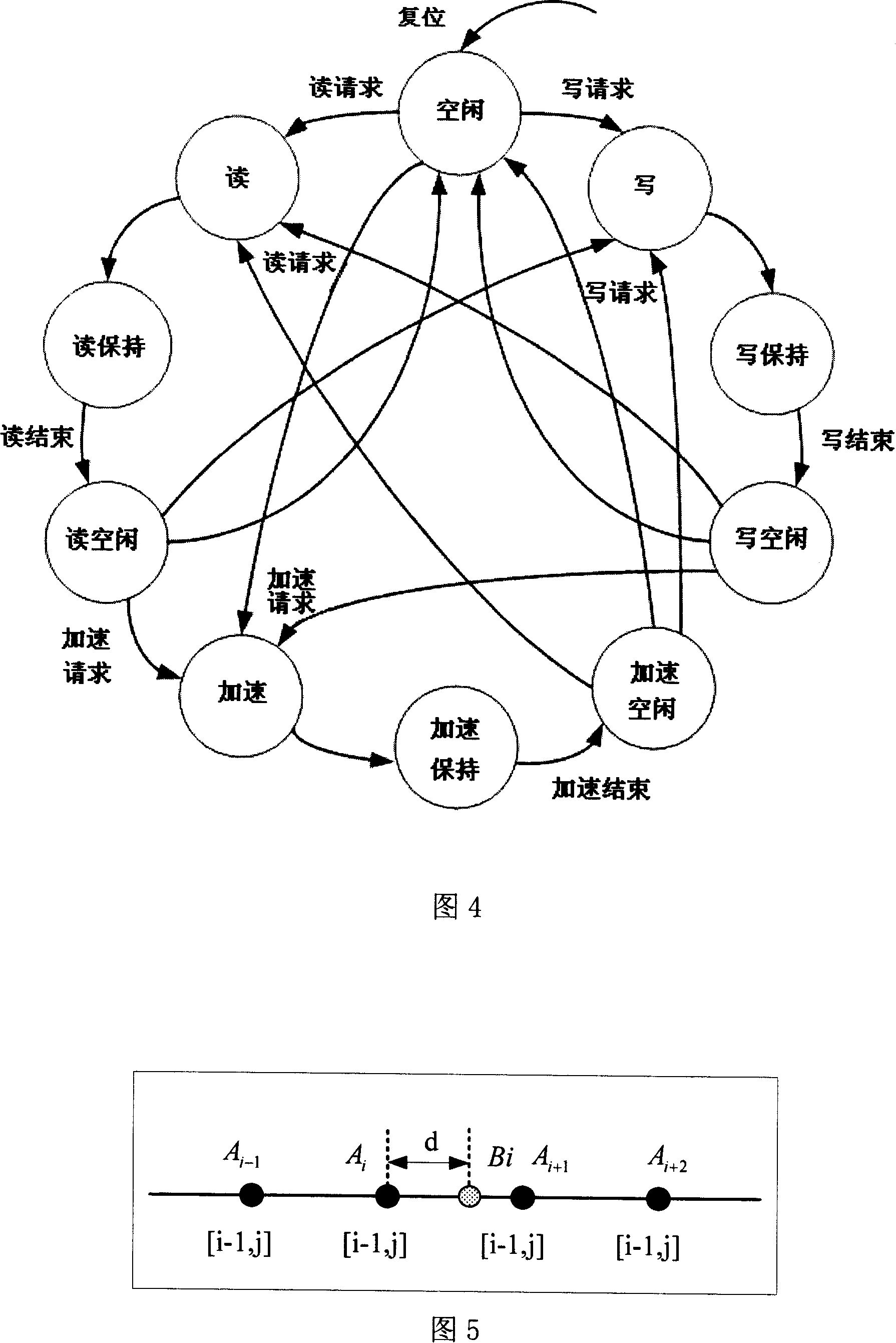
[0040] The storage operation c...
PUM
 Abstract
Description
Claims
Application Information