Method for clearing pollutant on standard wafer surface and emendation method for depth-measuring device

A technology for standard wafers and pollutants, applied in cleaning methods and tools, chemical instruments and methods, semiconductor/solid-state device testing/measurement, etc., can solve problems such as inability to accurately reflect the stability of testing equipment, unstable thickness testing results, etc. , to achieve the effect of maintaining stability and simple process

Inactive Publication Date: 2008-04-02
SEMICON MFG INT (SHANGHAI) CORP +1
View PDF1 Cites 10 Cited by
  • Summary
  • Abstract
  • Description
  • Claims
  • Application Information

AI Technical Summary

Problems solved by technology

[0008] The problem solved by the present invention is that the standard wafer in the prior art continuously absorbs pollutant particles in the environment, resulting in a continuous increase in thickness, resulting in unstable thickness detection results, which cannot accurately reflect the defects of the stability of the detection equipment

Method used


Image

  • Method for clearing pollutant on standard wafer surface and emendation method for depth-measuring device
  • Method for clearing pollutant on standard wafer surface and emendation method for depth-measuring device
  • Method for clearing pollutant on standard wafer surface and emendation method for depth-measuring device

Examples


Embodiment 1

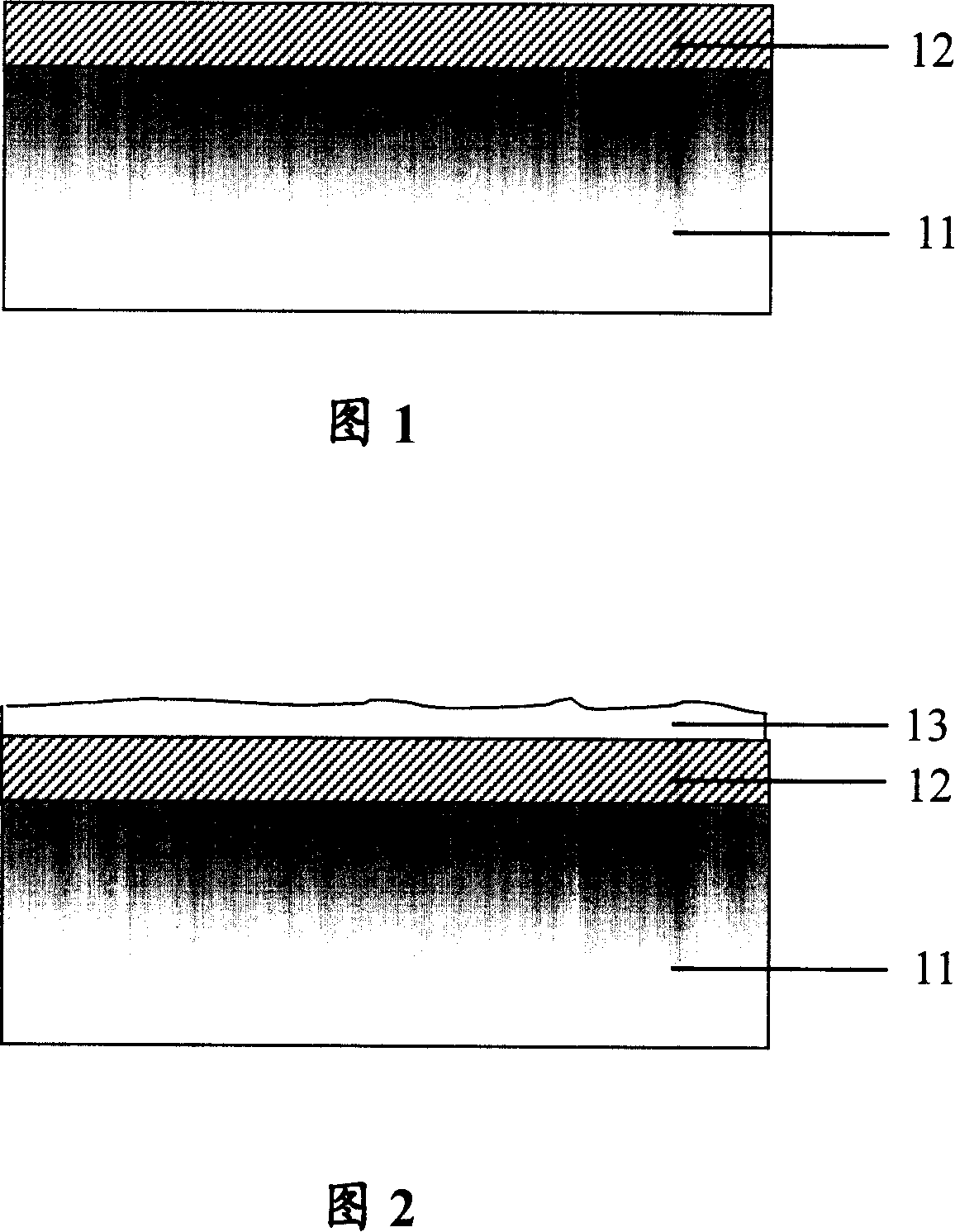
[0031] Referring to the accompanying drawing 1, it is a schematic diagram of the structure of a standard wafer. Among the figures, 11 is a semiconductor substrate. The standard wafer 11 can be a blank wafer or can be positioned at any stage of the semiconductor manufacturing process but has silicon oxide formed on its surface. Layer wafers, such as wafers with multiple film layers or multiple device layers but the surface layer is a silicon oxide layer. The wafer is pure semiconductor silicon or doped semiconductor silicon, and may also be semiconductor materials such as silicon-on-insulator or germanium. 12 is a film layer on the semiconductor substrate, and the film layer 12 can be various insulating materials such as oxides, nitrides, and oxynitrides, and can also be semiconductor materials such as polycrystalline silicon and monocrystalline silicon. The present invention is more suitable for The most important are insulating materials such as oxides such as silicon oxide. ...

Embodiment 2

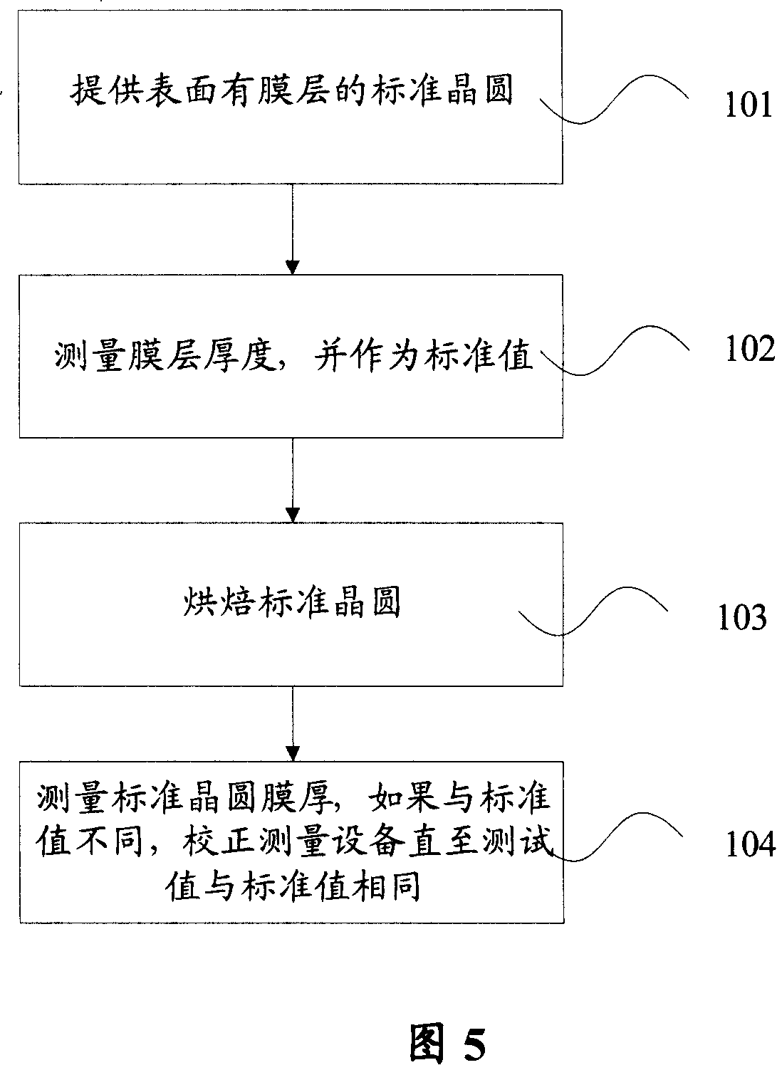
[0047] The present invention also provides a method for calibrating film thickness measuring equipment, comprising the following steps, referring to accompanying drawing 5, step 101, providing a standard wafer, the surface of the standard wafer has a film layer; step 102, detecting the film thickness and set it as a standard value; step 103, bake the standard wafer at a temperature of 50°C to 350°C; step 104, calibrate the film thickness measurement equipment, and place the baked standard wafer into The film layer measuring equipment measures its thickness, if the measured thickness does not match the standard value, correct the film layer thickness measuring device until the measured thickness is the same as the standard value.

[0048] The standard wafer described in this embodiment refers to the description in Example 1. At first, the film thickness on the standard wafer is detected and set as a standard value. After that, the standard wafer is heated at 50°C to 350°C. Baki...


PUM


Abstract

The invention relates to a method of removing pollutant on the surface of the standard wafer. The surface of the standard wafer is provided with a membrane layer; the standard wafer is baked at a temperature of 50 DEGC to 350 DEGC , which can wipe off the pollutant particles on the surface of standard wafer and keep the measured value of the thickness of the membrane stable. The invention also provides a method for revising the equipment for measuring the thickness of the membrane; the influence of the change of the thickness of the standard wafer on the measuring result, which ensures the accuracy and stability of the measuring result and is favorable to detecting the change of the performance of the membrane measuring equipment.

Description

technical field [0001] The invention relates to semiconductor technology, in particular to a method for removing pollutants on the surface of a standard wafer and a calibration method for thickness measuring equipment. Background technique [0002] With the continuous development of the semiconductor industry, the semiconductor manufacturing process has entered the nanometer era. In order to adapt to the trend of smaller and smaller electronic products and stronger functions, the line width in the semiconductor manufacturing process has also been developed from the original 0.18 micron to the present. 0.13 micron or even 90nm process. Along with the trend of chip functions becoming more powerful and components becoming smaller and smaller, the technical requirements for various links in the manufacturing process are getting higher and higher. Due to the smaller and smaller components and the more complex internal circuits, the process is more sensitive to subtle changes in ...

Claims


Application Information

Patent Timeline
Patent Type & Authority Applications(China)
IPC IPC(8): H01L21/00H01L21/66B08B7/00
Inventor 王小勇严博陈淑美吕秋玲
Owner SEMICON MFG INT (SHANGHAI) CORP
Why Eureka
Try Eureka