Preparation method of silicon transistor on source body Ohm contacting isolator

A silicon-on-insulator and ohmic contact technology, which is applied in semiconductor/solid-state device manufacturing, electrical components, circuits, etc., can solve the problems of reducing circuit speed and increasing circuit dynamic power consumption, so as to reduce dynamic power consumption and reduce leakage-induced potential Barrier lowering effect, effect of improving breakdown voltage

Inactive Publication Date: 2008-04-16
INST OF MICROELECTRONICS CHINESE ACAD OF SCI
View PDF0 Cites 4 Cited by
  • Summary
  • Abstract
  • Description
  • Claims
  • Application Information

AI Technical Summary

Problems solved by technology

However, these two structures increase the gate capacitance of the device, severely reduce the speed of the circuit, and increase the dynamic power consumption of the circuit

Method used


Image

  • Preparation method of silicon transistor on source body Ohm contacting isolator
  • Preparation method of silicon transistor on source body Ohm contacting isolator
  • Preparation method of silicon transistor on source body Ohm contacting isolator

Examples


Embodiment Construction

[0033] In order to make the objectives, technical solutions, and advantages of the present invention clearer, the following further describes the present invention in detail in conjunction with specific embodiments and with reference to the accompanying drawings.

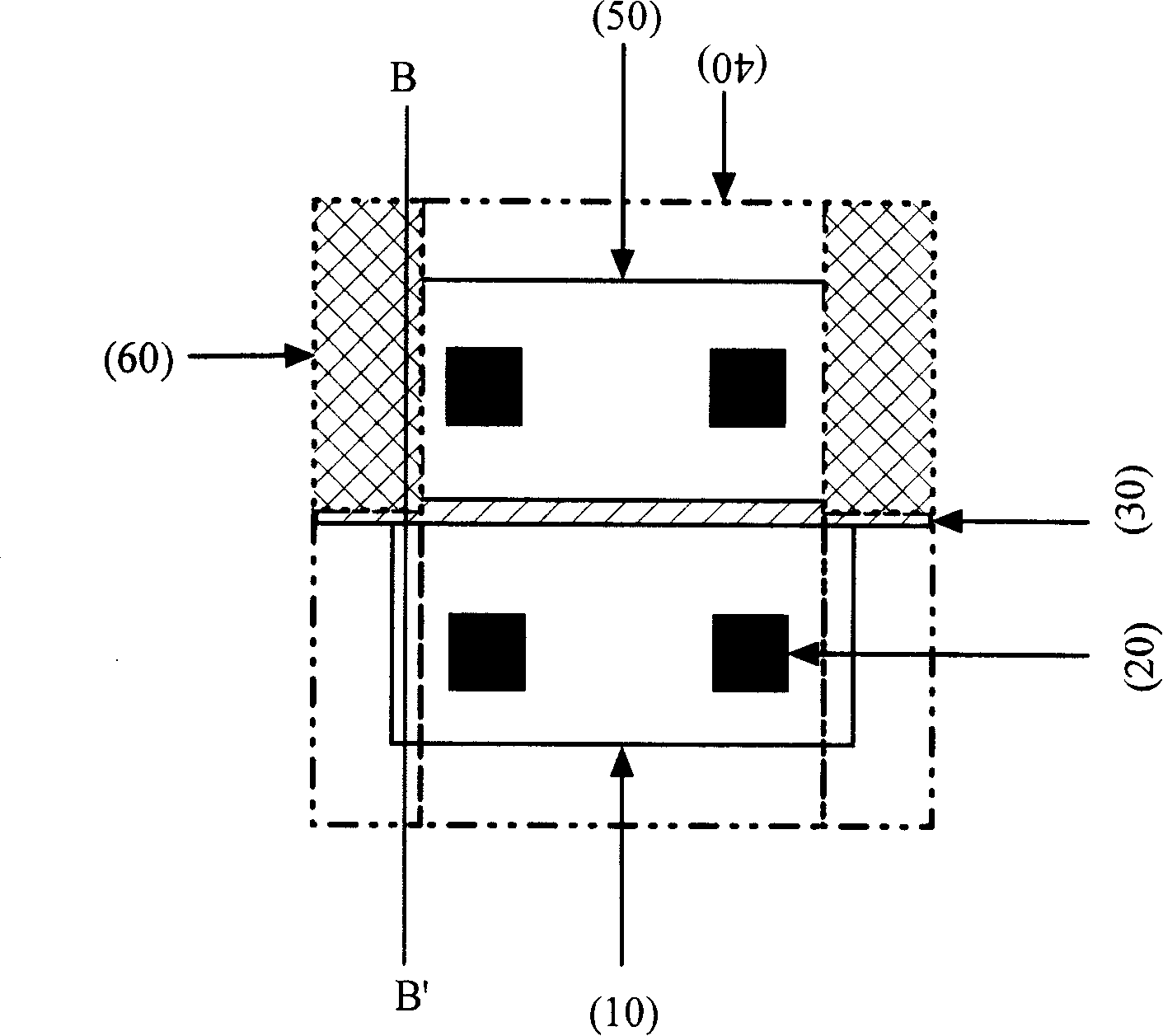
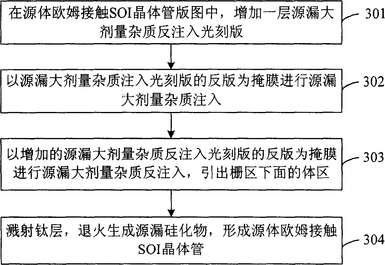
[0034] The working principle of the source-body ohmic contact SOI transistor of the present invention is that a layer of source-drain high-dose impurity back-injection photolithography plate 60 is added to the source-body ohmic contact SOI transistor layout; the photolithography plate 40 is used as a mask. Source and drain high-dose impurity implantation; source and drain high-dose impurity back-implantation of the photolithography plate 60 as a mask for source-drain high-dose impurity back implantation to lead out the body region 54 under the gate; sputtering titanium layer, annealing The source and drain silicides fix the body region and the source region at the same potential, thus eliminating the floating body effec...


PUM

PropertyMeasurementUnit
Thicknessaaaaaaaaaa

Abstract

The invention discloses a method for manufacturing source ohmic contact SOI transistor. The method comprises: A. a layer of source-drain photoetching model with megadose impurity reversely injected is added in the model of the source ohmic contact SOI transistor; B. the reverse model of the source-drain photoetching model with megadose impurity injected is taken as the mask to do the injection of source-drain megadose impurity; C. the reverse model of the added source-drain photoetching model with megadose impurity reversely injected is taken as the mask to do the reverse injection of source-drain megadose impurity and to draw out the body area under the grid area; D. sputtering titanic layer is generated into source-drain silicide by anneal means to form a source ohmic contact SOI transistor. The invention is adopted to eliminate the phenomenon of fringe electric leakage and the floating-body effect existing in the partial depletion of the SOI floating-body device. The invention is completely compatible with the technique of CMOS field effect transistor, thereby the invention is suitable for the IC field with low voltage, low power consumption and high reliability and can be used for the commercial production.

Description

Technical field [0001] The invention relates to the technical field of semiconductor device manufacturing, in particular to a method for manufacturing a source body ohmic contact silicon-on-insulator (SOI) transistor. Background technique [0002] SOI technology is recognized as one of the mainstream semiconductor technologies in the 21st century, and it is very likely to replace bulk silicon as the first choice for CMOS processes. Generally speaking, compared to bulk silicon devices, SOI devices have the advantages of small parasitic capacitance, low power consumption, fast speed, and no latch-up effect. In particular, SOI devices are more able to cope with various harsh environment challenges, such as radiation. surroundings. [0003] SOI is classified into partially depleted SOI (PDSOI) and fully depleted SOI (FDSOI) according to the thickness of the top silicon film. Because fully depleted SOI devices have technical difficulties such as difficulty in controlling the threshold...

Claims


Application Information

Patent Timeline
IPC IPC(8): H01L21/336
Inventor 毕津顺海潮和
Owner INST OF MICROELECTRONICS CHINESE ACAD OF SCI
Why Eureka
Try Eureka