High power semiconductor laser device coupling packaging component

A technology for packaging components and lasers, which is applied to semiconductor lasers, structural details of semiconductor lasers, laser components, etc., can solve problems such as low fiber coupling efficiency, low power density, and laser damage, so as to improve fiber coupling efficiency and reduce reflection The influence of light, the effect of ensuring work stability

Inactive Publication Date: 2008-04-16
BUTTERFLY TECH SHENZHEN
View PDF0 Cites 8 Cited by
  • Summary
  • Abstract
  • Description
  • Claims
  • Application Information

AI Technical Summary

Problems solved by technology

[0003] The coupling package form of the above-mentioned laser components has the following disadvantages: (1) The divergence angle of the laser in the C-Mount package is large (the divergence angle in the horizontal direction is 8°-10°, and the divergence angle in the vertical direction is 35°-40°), and the power The density is small, and the fiber coupling efficiency is low; (2) the end of the multimode fiber 3 is very close to the laser light-emitting chip, and the laser light-emitting chip is easily damaged during fiber coupling; (3) when the laser is coupled into the end face of the multimode fiber 3, the multimode The reflected light generated by the end face of the fiber 3 will be reflected to the light-emitting chip of the C-Mount packaged laser, which will affect the stability of the laser and cause damage to the laser

Method used


Image

  • High power semiconductor laser device coupling packaging component
  • High power semiconductor laser device coupling packaging component

Examples


Embodiment Construction

[0019] The present invention will be further described below in conjunction with the accompanying drawings and specific embodiments.

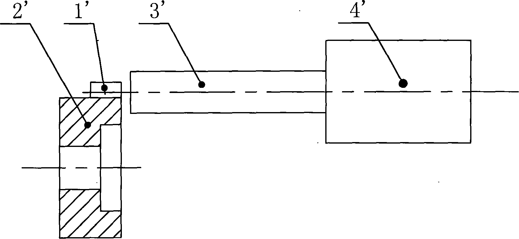
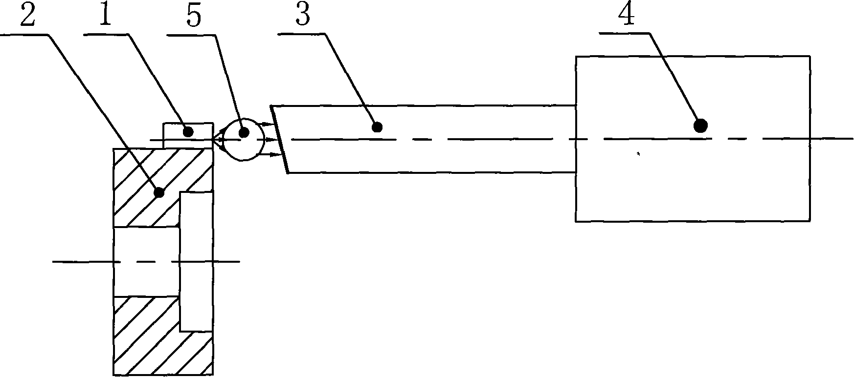
[0020] refer to figure 2 As shown, a high-power semiconductor laser coupling package assembly includes a C-Mount package laser emitting laser, a transmission fiber 3 and an optical fiber connector 4, and the C-Mount package laser includes a heat sink 2 and is fixed on the heat sink The laser light-emitting chip 1 on 2 and the fiber connector 4 are connected to one end of the transmission fiber 3. The laser light emitted by the laser light-emitting chip 1 is coupled into the transmission fiber 3 and then output from the fiber connector 4 at one end of the transmission fiber 3. Among them, a cylindrical lens 5 is arranged between the emitting end of the laser (that is, the light-emitting end of the laser light-emitting chip 1), the end of the transmission fiber 3 and the laser coupling, and the cylindrical lens 5 is used to compress the laser li...


PUM


Abstract

The present invention discloses a large power semiconductor laser coupling encapsulation component, which comprises a C-Mount encapsulation laser for emitting laser, a transmitting optical fiber coupled with emitted laser, an optical fiber connecting head for outputting laser and connected with the transmitting optical fiber and a pillar lens which is arranged between the emitting end of the laser and the transmitting optical fiber for compressing laser. An inclined plane is formed on the coupled end of the transmitting optical fiber and the laser. An AR film is coated on the inclined plane. The coupling encapsulation form of the C-Mount encapsulation laser has the advantages of (1) high coupling efficiency of the optical fiber, (2) no influence on working stability of laser without reflection on the light emitting chip of the laser from the reflecting light on the end face of the transmitting optical fiber and (3) no damage on the light emitting chip of the laser during coupling of the optical fiber due to moderate distance between the end face of the transmitting optical fiber and the end face of the light emitting chip of the laser.

Description

technical field [0001] The invention relates to the technical field of semiconductor lasers, in particular to a coupling package assembly of high-power semiconductor lasers. Background technique [0002] Existing high-power semiconductor lasers, such as C-Mount packaged laser components, are mainly formed by directly coupling and packaging the laser light-emitting chip fixed on the heat sink and the multimode fiber with the SMA905 fiber connector. Its specific structure is as figure 1 As shown, the laser light-emitting chip 1' is fixed on the heat sink 2', the multimode fiber 3' is placed in front of the emitting end of the laser light-emitting chip 1', and the laser light emitted by the laser light-emitting chip 1' is coupled into the multimode fiber 3' At one end, the other end of the multimode optical fiber 3' is connected with an SMA905 optical fiber connector 4' for outputting laser light. [0003] The coupling package form of the above-mentioned laser components has ...

Claims


Application Information

Patent Timeline
Patent Type & Authority Applications(China)
IPC IPC(8): H01S5/00H01S5/02G02B6/42G02B6/00
Inventor 付树阶宋焕玉
Owner BUTTERFLY TECH SHENZHEN
Why Eureka
Try Eureka