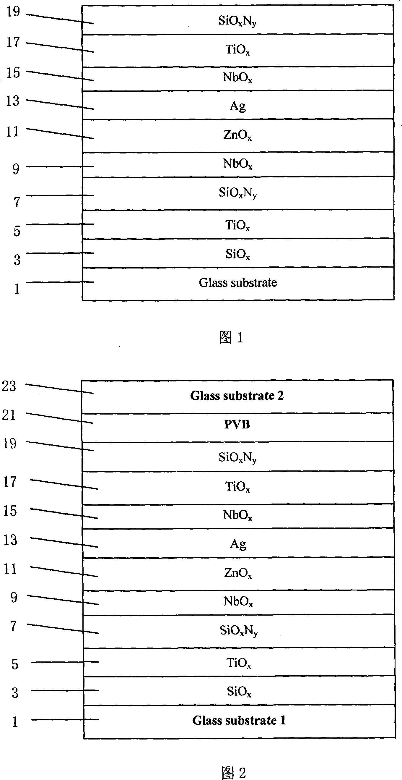
Low radiation coated glass capable of being bended by baking
A low-emissivity coating and bending technology, applied in the field of coated glass, can solve the problem that the film layer cannot withstand high temperature for a long time, achieve a unique heat insulation effect, save heating costs, and save cooling costs
- Summary
- Abstract
- Description
- Claims
- Application Information
AI Technical Summary
Problems solved by technology
Method used
Image
Examples
Embodiment 1
[0037] The first dielectric layer is plated on the clean float glass original sheet with a thickness of 1.8 mm after washing, polishing, and drying, that is, SiO is plated in sequence. x / TiO x / SiO x N y / NbO x / ZnO x film layer, which is coated with SiO x 、TiO x , SiO x N y The other film layer uses a rotating target, plated with NbO x The target used for the film layer is a planar target, ZnO x The film layer uses a rotating target; where,
[0038] SiO x In the film layer, x=0.8, and the film thickness is 19nm;
[0039] TiO x In the film layer, x=1.2 and the thickness is 13nm;
[0040] SiO x N y In the film layer, x=0.5, y=1, and the thickness is 30nm;
[0041] NbO x In the film layer, x=2 and the thickness is 10nm;
[0042] ZnO x In the film layer, x=0.6, and the thickness is 8nm.
[0043] Secondly, a low-emissivity film layer, ie, an Ag layer, is coated. The target material used is a planar target, and the thickness of the film layer is 7nm.
[0044] ...
Embodiment 2
[0054] On the clean original float glass with a thickness of 2.1mm after washing, polishing and drying, SiO2 is plated in sequence. x / SiO x N y / SnO x / NiCrO x / ZnSnO x / Ag / NiCrO x / SnO x / SiO x N y film layer, of which:
[0055] SiO x In the film layer, x=1.4, and the film thickness is 22nm;
[0056] SiO x N y In the film layer, x=1.5, y=0.33, and the thickness is 26nm;
[0057] SnO x In the film layer, x=0.7 and the thickness is 11nm;
[0058] NiCrO x In the film layer, x=1 and the thickness is 13nm;
[0059] ZnSnO x In the film layer, x=0.4, and the thickness is 12nm.
[0060] Secondly, a low-radiation film layer, ie, an Ag layer, is plated on, and the thickness of the film layer is 17nm.
[0061] Then the second dielectric layer is plated, and NiCrO is plated in sequence x / SnO x layer;
[0062] NiCrO x In the film layer, x=1.6 and the thickness is 15nm;
[0063] SnO x In the film layer, x=1.3, and the thickness is 26nm.
[0064] Finally, a prote...
PUM
| Property | Measurement | Unit |
|---|---|---|
| thickness | aaaaa | aaaaa |
| thickness | aaaaa | aaaaa |
| thickness | aaaaa | aaaaa |
Abstract
Description
Claims
Application Information
