
Multicrystalline silicon compounds electric fuse silk part

A technology of silicided electricity and polysilicon, which is applied to electric solid devices, electrical components, semiconductor devices, etc., can solve the problems of increased resistance at both ends of fuses, unstable recrystallization of polysilicon, and alignment errors affecting the size of three polysilicon regions.

Active Publication Date: 2008-04-30
SHANGHAI HUAHONG GRACE SEMICON MFG CORP
View PDF2 Cites 18 Cited by
  • Summary
  • Abstract
  • Description
  • Claims
  • Application Information

AI Technical Summary

Problems solved by technology

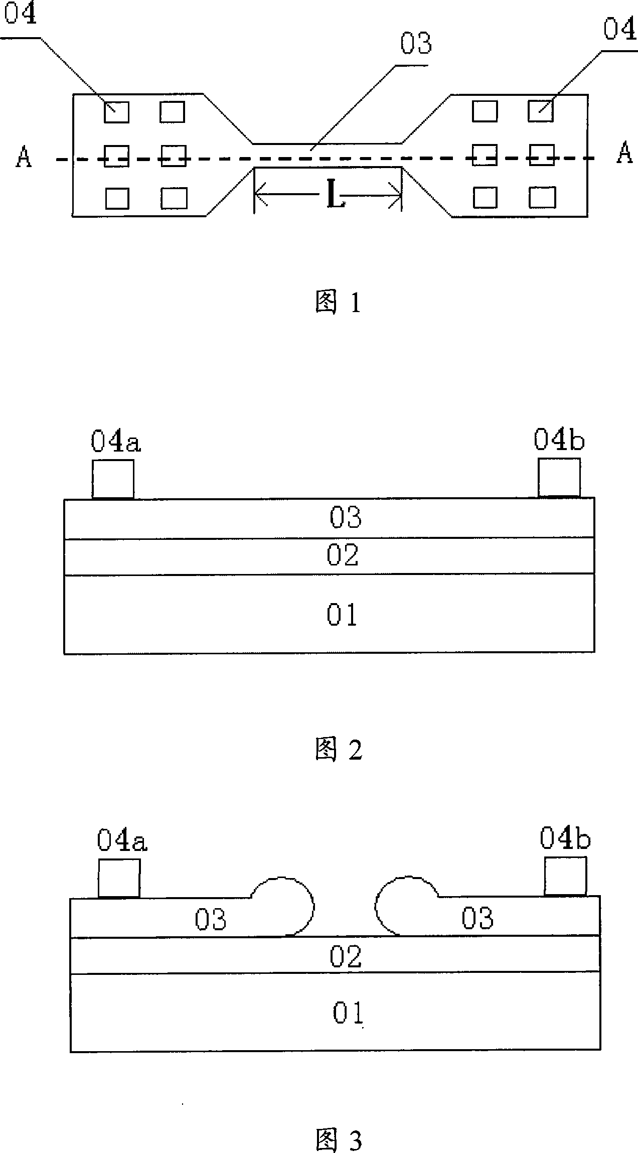
At the same time, the heat generated by the transient large current will also recrystallize the polysilicon and redistribute the impurities under the fuse area, which will significantly increase the resistance of the two terminals 04a and 04b of the fuse
[0004] With the improvement of integrated circuit technology and the continuous shrinking of device size, the above-mentioned similar fuse structures have the following disadvantages: First, there are residual silicide fuses after voltage fusing, or the recrystallization of polysilicon is unstable, resulting in an increase in the distribution range of resistance values ​​after fusing. The maximum and median (mean) are small; the second is that the high heat generated by the current fed by the fuse will cause overheating of the surrounding devices on the chip, thereby reducing the stability of the device
However, two layers of ion implantation masks are required in the manufacturing process. The alignment error of the two layers of masks affects the size of the three polysilicon regions, which in turn affects the uniformity of the resistance value after fusing.

Method used


Image

  • Multicrystalline silicon compounds electric fuse silk part
  • Multicrystalline silicon compounds electric fuse silk part
  • Multicrystalline silicon compounds electric fuse silk part

Examples


Embodiment Construction

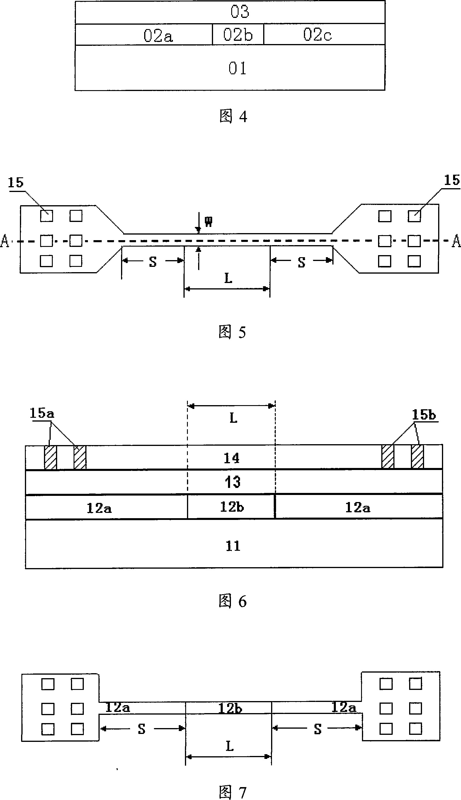
[0032] As shown in Figure 5 and Figure 6, a polysilicon silicide electric fuse device includes:

[0033] substrate 11,

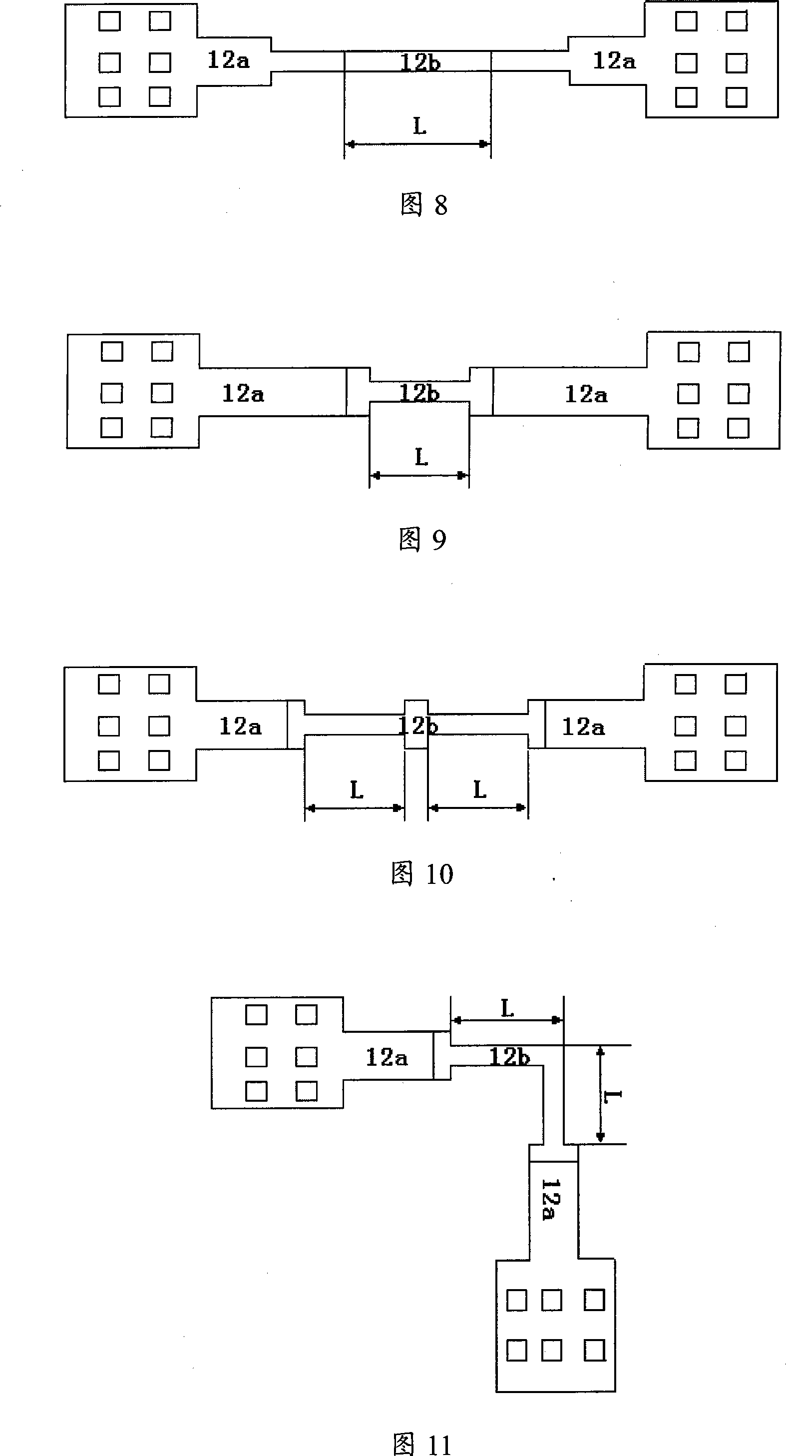
[0034] A semiconductor material layer 12 disposed on the substrate 11, the semiconductor material layer 12 includes lead-out regions 12a with the same type of doping at both ends and an undoped region in the middle or a middle region 12b with a lower doping concentration than the lead-out regions at both ends ; There are one or more fusing zones L in the middle zone 12b;

[0035] A metal silicide layer 13 disposed on the semiconductor material layer 12 .

[0036] Wherein, the metal silicide layer 13 is also provided with a dielectric layer 14, and the lead-out regions 12a at both ends of the dielectric layer 14 are respectively provided with one or more contact holes 15 penetrating to the metal silicide layer 13. .

[0037] Wherein, the semiconductor material layer 12 may be selected from one of semiconductor materials such as polysilicon, amorphous silic...


PUM


Abstract

A polycide electric fuse device includes an underlay, and a semiconductor material layer arranged on the underlay. The semiconductor material layer includes an outgoing area with the same doping sorts on two ends and a middle undoped area or a middle area with the doping content lower than two ends of the outgoing area. The middle area is provided with one or a plurality of blowing areas. A metal silicide layer is arranged on the semiconductor material layer. The invention will control the blowing within the undoped or less doped middle area. After blowing, resistance medium value increases and distribution range narrows down. The invention also can prohibit the area overheating caused by current in blowing.

Description

technical field [0001] The invention relates to an electric fuse device used in a semiconductor integrated circuit, in particular to a novel electric fuse structure composed of polysilicon and metal silicide. Background technique [0002] Electric fuse is a commonly used device for semiconductor integrated circuits. It is a low-resistance connection line. After being burned by high voltage, the resistance becomes very large, that is, the equivalent connection line is disconnected. It has two main purposes. One is to connect redundant circuits. When the detection circuit detects damaged devices or circuit units in the circuit, these connecting lines are fused by applying a higher voltage to select redundant units with the same function to replace them. The other is used for the programming function of the integrated circuit, that is, the circuit, the device array and the programming circuit are processed on the chip first, and then the data is input from the outside, and the ...

Claims


Application Information

Patent Timeline
Patent Type & Authority Applications(China)
IPC IPC(8): H01L23/58H01L23/62H01L27/04
CPCH01L23/5256H01L2924/0002H01L2924/00
Inventor 高文玉韦敏侠李睿王庆东
Owner SHANGHAI HUAHONG GRACE SEMICON MFG CORP
Learn More