Packaging structure and method for manufacturing the packaging structure

A technology of packaging structure and manufacturing method, applied in semiconductor/solid-state device manufacturing, electrical components, electrical solid-state devices, etc., can solve problems such as products and methods that do not have suitable structures and methods, affect the quality of packaging structures, and reduce chip quality, etc. Achieve the effect of saving material cost, reducing volume and improving quality

Active Publication Date: 2008-05-21
ADVANCED SEMICON ENG INC
View PDF0 Cites 16 Cited by
  • Summary
  • Abstract
  • Description
  • Claims
  • Application Information

AI Technical Summary

Problems solved by technology

However, every semiconductor chip will inevitably generate electromagnetic radiation during operation. With the miniaturization of the packaging structure, this method of integrating multiple semiconductor packages into a single packaging structure can greatly reduce the The distance between chips, but this highlights the problem of mutual interference between different chips
In a packaging structure with high component density, multiple semiconductor chips that interfere with each other not only reduce the quality of chip operation, but also increase the noise value of the overall packaging structure, affecting the quality of the entire packaging structure
[0004] It can be seen that the above-mentioned existing packaging structure and its manufacturing method obviously still have inconvenience and defects in product structure, manufacturing method and use, and need to be further improved urgently.
In order to solve the above-mentioned problems, the relevant manufacturers have tried their best to find a solution, but no suitable design has been developed for a long time, and there is no suitable structure and method for general products and methods to solve the above-mentioned problems. This is obviously a problem that relevant industry players are eager to solve

Method used


Image

  • Packaging structure and method for manufacturing the packaging structure
  • Packaging structure and method for manufacturing the packaging structure
  • Packaging structure and method for manufacturing the packaging structure

Examples


no. 1 example

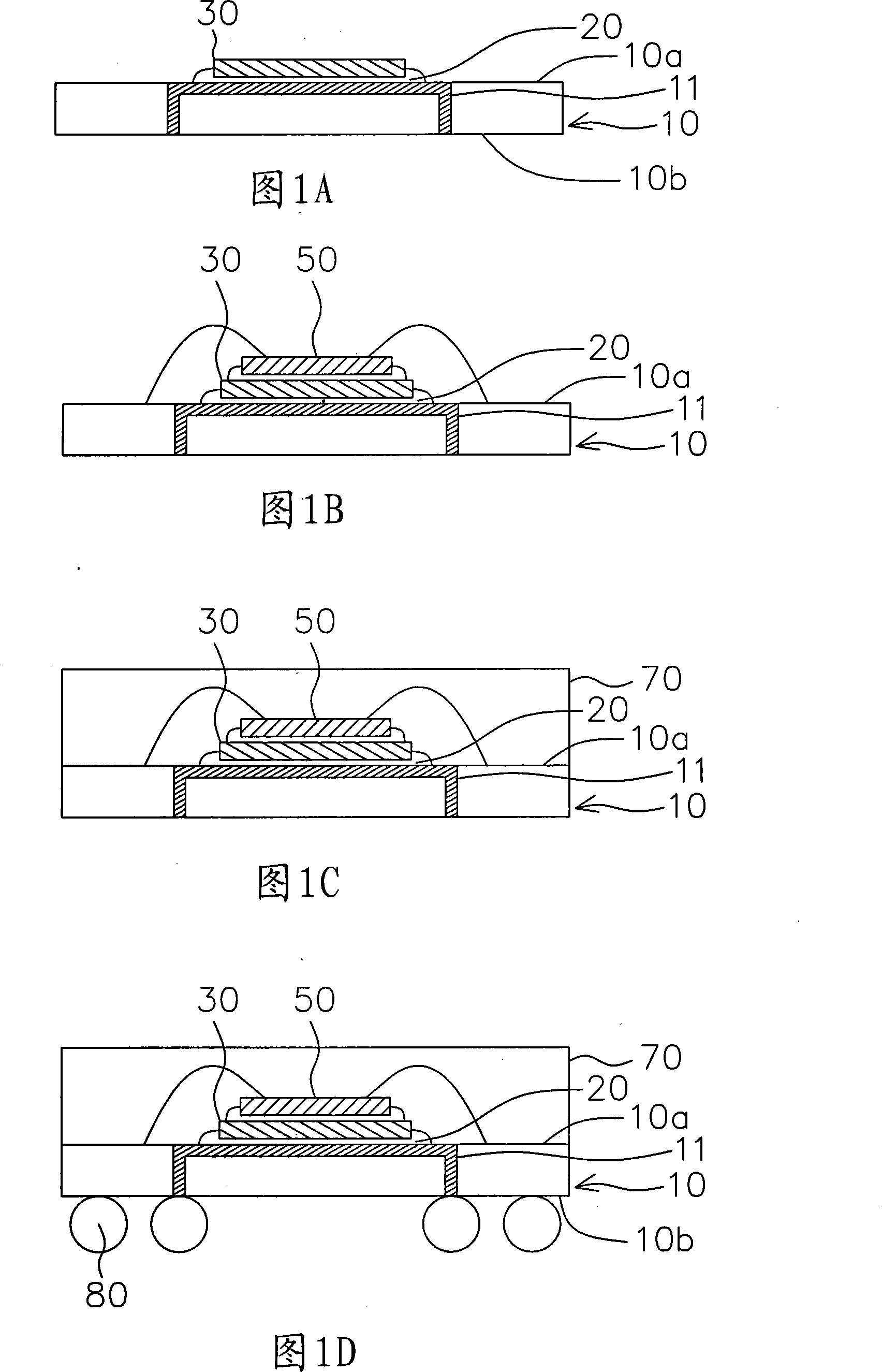
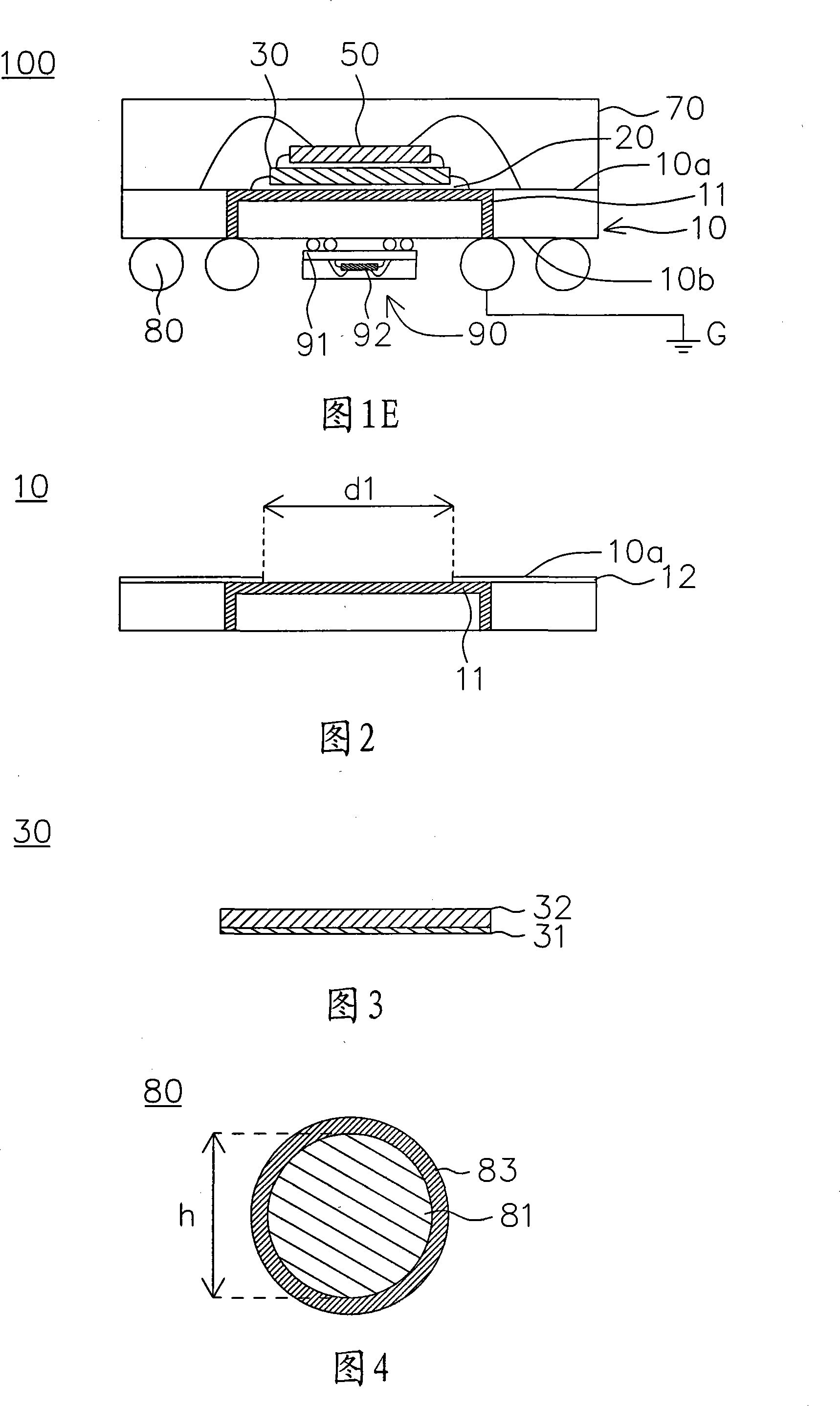
[0054] Please refer to FIGS. 1A to 1E at the same time. FIG. 1A is a schematic diagram showing a substrate and a shielding element according to a first embodiment of the present invention, and FIG. 1B is a schematic diagram showing a shielding element disposed on the substrate of FIG. 1A. 1C is a schematic diagram showing a chip disposed on the shielding element of FIG. 1B, FIG. 1D is a schematic diagram showing a sealant layer formed on the substrate of FIG. 1C, and FIG. 1E is a schematic diagram showing a package according to the first embodiment of the present invention Schematic diagram of the structure.

[0055] The manufacturing method of the package structure according to the first embodiment of the present invention includes the following steps:

[0056] First, a substrate 10 is provided, and a shielding element 30 is arranged on the substrate 10. Please refer to FIG. 1A, the substrate 10 has a first surface 10a and a second surface 10b, and the first surface 10a is opposi...

no. 2 example

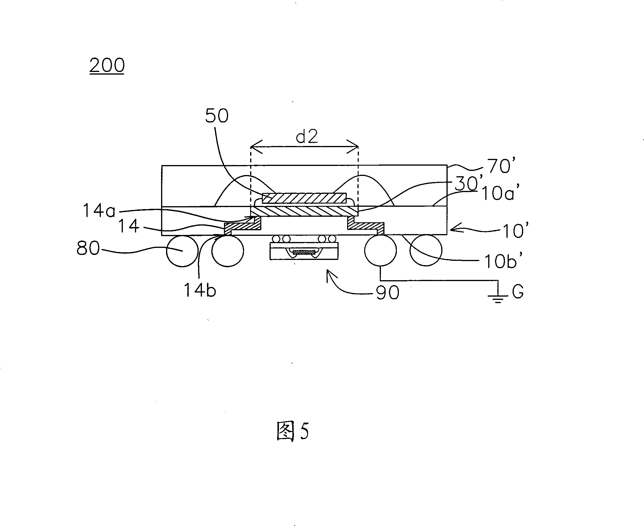
[0075]Please refer to FIG. 5, which is a schematic structural diagram of the package structure according to the second embodiment of the present invention. The package structure 200 of the second embodiment of the present invention includes a substrate 10', a chip 50, an encapsulant layer 70' and a semiconductor device 90. The package structure 200 of this embodiment is different from the package structure 100 according to the first embodiment of the present invention. The difference lies in the position of a shielding element 30' relative to the substrate 10', and the shielding element 30' is connected to a solder ball 80 The other similarities will be omitted here and will not be repeated here.

[0076] In this embodiment, the aforementioned substrate 10' has a first surface 10a' and an opposite second surface 10b', and the substrate 10' includes a shielding element 30'. The shielding element 30' is embedded in the substrate 10', and the first surface 10a' has an opening d2 to e...


PUM


Abstract

A package structure including a substrate, a shielding element, a chip, a sealant layer and a semiconductor device is provided. The substrate has a first surface and a second surface opposite to the first surface. The shielding element is disposed on the first surface. The chip is disposed on the shielding element and is electrically connected to the substrate. The sealant layer is disposed on the first surface, and encapsulates the chip and the shielding element. The semiconductor device is disposed on the second surface.

Description

Technical field [0001] The present invention relates to a packaging structure and a manufacturing method of the packaging structure, in particular to a method including a plurality of semiconductor chips, and a shielding element is arranged between the chip and the semiconductor device to shield the chip and the semiconductor device during operation. The resulting mutual electromagnetic interference phenomenon also has the advantages of improving operation stability, reducing volume, improving product quality, and saving development costs, and the packaging structure and the manufacturing method of the packaging structure. Background technique [0002] In order to meet the market's demand for highly integrated electronic products, the industry is committed to research and development and manufacture of consumer electronic products that are lighter in weight, smaller in size and more integrated with more functions. Therefore, it is necessary to add more equipment in the extremely ...

Claims


Application Information

Patent Timeline
Patent Type & Authority Applications(China)
IPC IPC(8): H01L25/00H01L23/552H01L23/488H01L23/31H01L21/50H01L21/60H01L21/56
CPCH01L2924/1532H01L2225/1058H01L2924/01082H01L2924/15174H01L24/48H01L25/105H01L24/32H01L2224/16H01L2224/48227H01L2924/01033H01L2225/1023H01L23/3128H01L2924/15311H01L23/552H01L2924/01075H01L2224/48091H01L2224/73265H01L2924/3025H01L2224/32225H01L2224/2612H01L2924/00014H01L2924/181H01L2924/00H01L2924/00012H01L2224/45099H01L2224/45015H01L2924/207
Inventor 李暎奎金烔鲁安载善车尚珍崔守珉
Owner ADVANCED SEMICON ENG INC
Why Eureka
Try Eureka