Ball grid array packaging substrate for enhancing spherical washer fixation and ball grid array packaging structure

An array packaging and fixation technology, which is applied in the field of ball grid array packaging substrate and ball grid array packaging structure, can solve the problems of increasing the ball pad area, affecting the circuit configuration of the ball grid array packaging substrate, and being unable to apply to the ball grid array packaging substrate. , to achieve a strong fixation effect

Inactive Publication Date: 2008-06-04
POWERTECH TECHNOLOGY
View PDF1 Cites 3 Cited by
  • Summary
  • Abstract
  • Description
  • Claims
  • Application Information

AI Technical Summary

Problems solved by technology

However, this method will greatly increase the area occupied by the ball pads on the surface of the substrate, and cannot be applied to high-density ball grid array packaging substrates.
Also, this affects the wiring configuration of the BGA substrate
[0006] It can be seen that the above-mentioned existing ball grid array packaging substrate obviously still has inconvenience and defects in struct...

Method used


Image

  • Ball grid array packaging substrate for enhancing spherical washer fixation and ball grid array packaging structure
  • Ball grid array packaging substrate for enhancing spherical washer fixation and ball grid array packaging structure
  • Ball grid array packaging substrate for enhancing spherical washer fixation and ball grid array packaging structure

Examples


no. 1 Embodiment

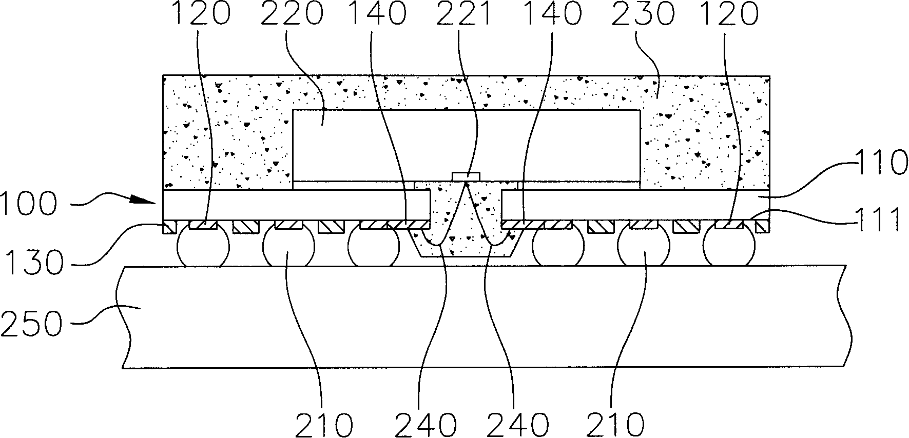
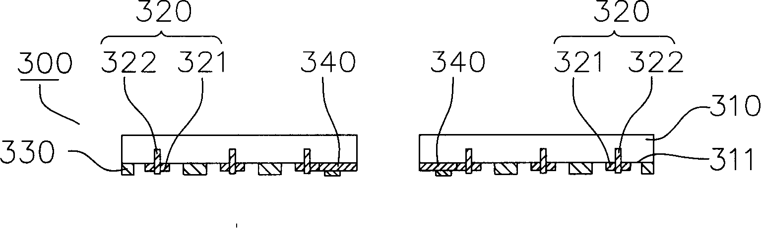
[0061] According to the first embodiment of the present invention, a ball grid array packaging substrate with enhanced ball pad fixation is disclosed, which is suitable for a chip carrier of semiconductor packaging. see image 3 Shown is a schematic cross-sectional view of a ball grid array packaging substrate that enhances the fixation of ball pads according to the first embodiment of the present invention. The BGA substrate 300 mainly includes a substrate core layer 310 , a plurality of ball pads 320 and a solder resist layer 330 . In this embodiment, the BGA substrate 300 has a single-layer wiring structure, which can be a printed circuit board, a ceramic carrier board or a circuit film. The arrangement of the ball pads 320 can be arrayed on the same surface of the substrate core layer 310 .

[0062] The substrate core layer 310 has a surface 311 on which circuits (not shown in the figure) can be arranged and a solder resist layer 330 is formed. Please refer to Figure ...

no. 2 Embodiment

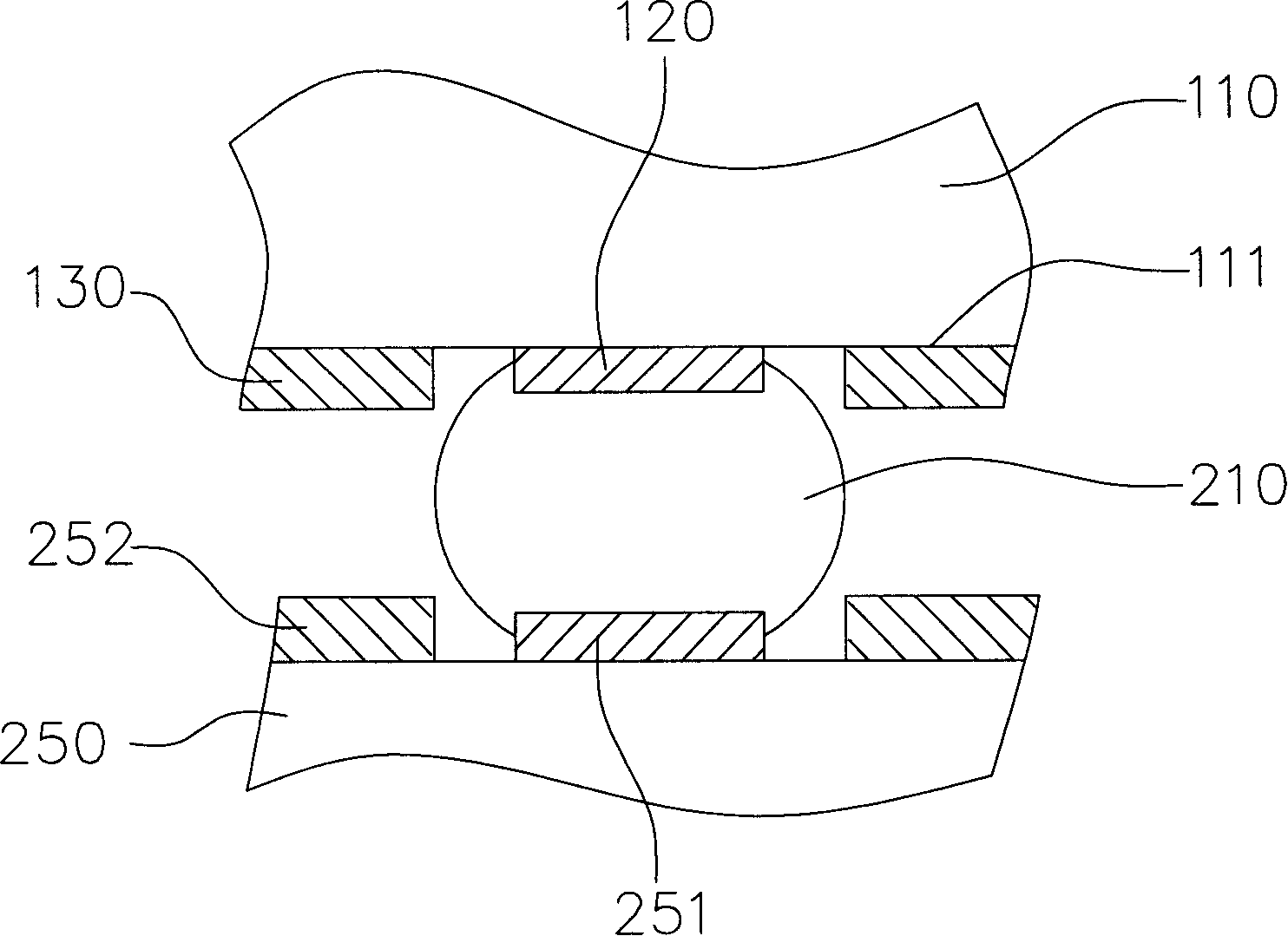
[0067] see Figure 6 As shown, the external printed circuit board 450 has a plurality of ball pads 451 exposed on the solder resist layer 452 thereof. The solder balls 410 bonded to the ball pads 320 are reflow bonded to the ball pads 451 . Since these ball pads 320 have strong fixation to the substrate core layer 310 and do not need to expand the area of ​​the surface 311 occupying the substrate core layer 310, the bonding interface is not easily affected by external forces and has separation or cracks. In the second specific embodiment, another ball grid array packaging substrate with enhanced fixation of the ball pads is disclosed to illustrate that the ball pads with special shapes can be optionally disposed. see Figure 7 Shown is a schematic cross-sectional view of another ball grid array packaging substrate that enhances the fixation of ball pads according to the second embodiment of the present invention. The BGA substrate 500 includes at least one substrate core la...


PUM


Abstract

The invention relates to an encapsulation substrate with a spherical lattice array for enhancing the fixation of a spherical pad and an encapsulation structure with the spherical lattice thereof. The encapsulation substrate with a spherical lattice array for enhancing the fixation mainly includes a core layer of the substrate, a plurality of spherical pads and an anti-wielding layer. Every spherical pad has a metal pad and at least a metal nail. The metal pad is clingingly arranged on a surface of the core layer of the substrate and the metal nail is embedded in the core layer of the substrate. The anti-wielding layer is formed on the core layer of the substrate and the metal pad is exposed. The encapsulation structure with the spherical lattice includes the encapsulation substrate with a spherical lattice array and a plurality of solder balls and the plurality of solder balls are conjugated with the spherical pads. By utilizing the shapes of the spherical pads in the invention, contact area for the core layer of the substrate can be increased to further prevent a conjunction interface between the metal pad and the core layer of the substrate from separating or cracking.

Description

technical field [0001] The invention relates to a circuit substrate suitable for semiconductor packaging, in particular to a ball grid array packaging substrate and a ball grid array packaging structure that enhance the fixation of ball pads. Background technique [0002] see figure 1 Shown is a schematic cross-sectional view of a conventional BGA structure after surface bonding. An existing conventional ball grid array packaging structure uses a ball grid array packaging substrate 100 as a chip carrier. The ball grid array packaging substrate 100 mainly includes a substrate core layer 110, a plurality of ball pads 120 and a solder resist layer 130. . The substrate core layer 110 has a surface 111 . The ball pads 120 are disposed on the surface 111 of the substrate core layer 110 . The solder resist layer 130 is formed on the surface 111 of the substrate core layer 110 and exposes the ball pads 120 . The lines 140 are disposed on the surface 111 of the substrate core la...

Claims


Application Information

Patent Timeline
IPC IPC(8): H01L23/498H01L23/488
CPCH01L2224/32225H01L2224/48091H01L2224/48227H01L2224/4824H01L2224/73215H01L2224/73265H01L2924/15311H01L2924/181
Inventor 范文正
Owner POWERTECH TECHNOLOGY
Why Eureka
Try Eureka