Wafer multi-test object parallel test system

A test system and test object technology, used in semiconductor/solid-state device testing/measurement, electronic circuit testing, single semiconductor device testing, etc., and can solve problems such as wafer fluctuation disturbance, unsolved wafer signal interference, distortion

Active Publication Date: 2008-06-11
SHANGHAI HUAHONG GRACE SEMICON MFG CORP
View PDF0 Cites 9 Cited by
  • Summary
  • Abstract
  • Description
  • Claims
  • Application Information

AI Technical Summary

Problems solved by technology

[0003] During the test process, the parallel test of multiple test objects is likely to cause fluctuations in the ground potential of the wafer. For some signal-sensitive wafer devices, such disturbances will lead to unstable or distorted test results during parallel testing.
[0004] In the prior art, the problem of crosstalk in parallel testing of multiple test objects is usually reduced by improving the signal shielding on the path from the probe to the ATE test channel, but this does not solve the problem of signal interference occurring on the wafer

Method used


Image

  • Wafer multi-test object parallel test system

Examples


Embodiment Construction

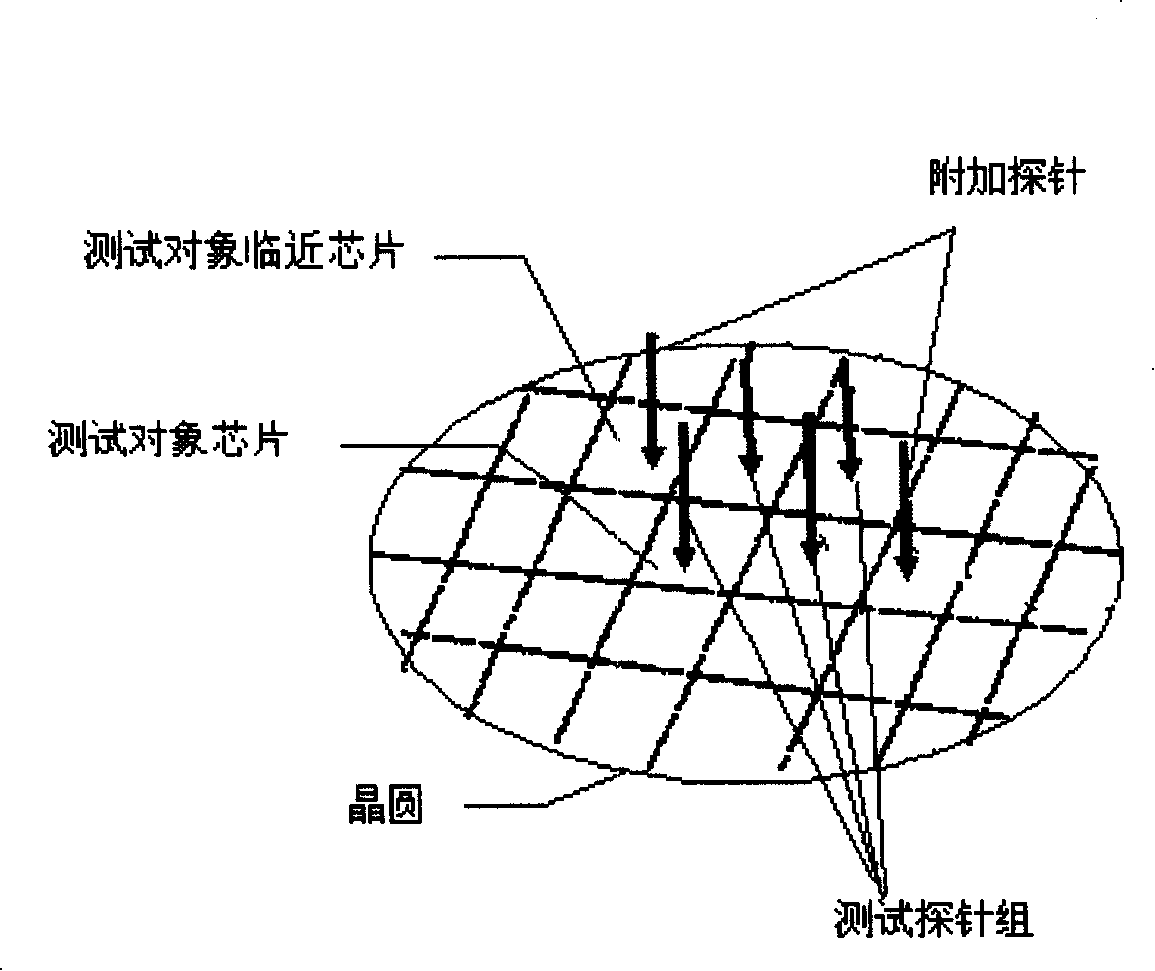
[0010] The invention reduces the test stability problem of the parallel test object caused by the fluctuation of the ground potential during the parallel test by enhancing the ground connection of the area near the test object on the wafer.

[0011] As shown in the figure, in addition to configuring the probe sets of multiple test objects required for parallel testing on the probe card, additional probes corresponding to the test objects adjacent to the chip are additionally configured. Ease of decision.

[0012] The type of chip pin terminal corresponding to the additional probe, first, consider the GND terminal (ground terminal) of the chip. If the chip does not have enough GND terminals, it can also correspond to ordinary signal terminals. On the probe card, additional probes can be connected directly to the tester's ground terminal or to the tester's test channel. If it is connected to the test channel, it needs to be set to the ground level by controlling the ATE through...


PUM


Abstract

The invention discloses a parallel test system of the wafer multiple test objects, which comprises a probe group of the multiple test objects that the parallel test requires, and the additional probes corresponding to the close chip of the test objects. The additional probes correspond to the ground terminal or other terminals of the close chip of the test objects, and contact with them when under test. The invention effectively solves the problem of crosstalk due to the leakage of charge pattern of the ground potential in the process of parallel test.

Description

technical field [0001] The invention relates to a test system for semiconductor integrated circuits, in particular to a parallel test system for wafers with multiple test objects. Background technique [0002] In the test of semiconductor integrated circuits, in order to improve the test efficiency, the method of parallel testing of multiple test objects is usually used in the wafer ATE test, that is, the probes corresponding to multiple test objects are arranged on the probe card, and the test passes The control of the test program realizes the parallel testing of multiple test objects of ATE (Automatic Test Equipment). [0003] During the test process, the parallel test of multiple test objects is likely to cause fluctuations in the ground potential of the wafer. For some signal-sensitive wafer devices, such disturbances will lead to unstable or distorted test results during parallel testing. [0004] In the prior art, the problem of crosstalk in parallel testing of multi...

Claims


Application Information

Patent Timeline
Patent Type & Authority Applications(China)
IPC IPC(8): G01R31/28G01R31/26G01R31/3193H01L21/66
Inventor 曾志敏
Owner SHANGHAI HUAHONG GRACE SEMICON MFG CORP
Why Eureka
Try Eureka