Pixels array module group and flat display device

A pixel array, flat display technology, applied in identification devices, optics, instruments, etc., can solve problems such as inability to use small-sized substrates for splicing, inconvenience, and use of display surfaces.

Inactive Publication Date: 2008-06-25
GIGNO TECH CO LTD
View PDF0 Cites 8 Cited by
  • Summary
  • Abstract
  • Description
  • Claims
  • Application Information

AI Technical Summary

Problems solved by technology

[0006] However, the above two structures require reserved space to connect the drive circuit or set the drive chip. Dimensions of the substrate spliced ​​together
Directly producing large-sized substrates will require more process equipment, and whenever there is a new size requirement, different process equipment is required to meet it, which is really uneconomical and costly.
[0007] This shows that the above-mentioned existing flat display device obviously still has inconvenience and defects in structure and use, and needs to be further improved urgently.
In order to solve the problems of flat panel display devices, relevant manufacturers have tried their best to find a solution, but no suitable design has been developed for a long time, and there is no suitable structure for general products to solve the above problems, which is obvious. It is a problem that relevant industry players are eager to solve

Method used


Image

  • Pixels array module group and flat display device
  • Pixels array module group and flat display device
  • Pixels array module group and flat display device

Examples


Embodiment Construction

[0064] In order to further explain the technical means and effects of the present invention to achieve the intended purpose of the invention, below in conjunction with the accompanying drawings and preferred embodiments, the specific implementation, structure, Features and their functions are described in detail below.

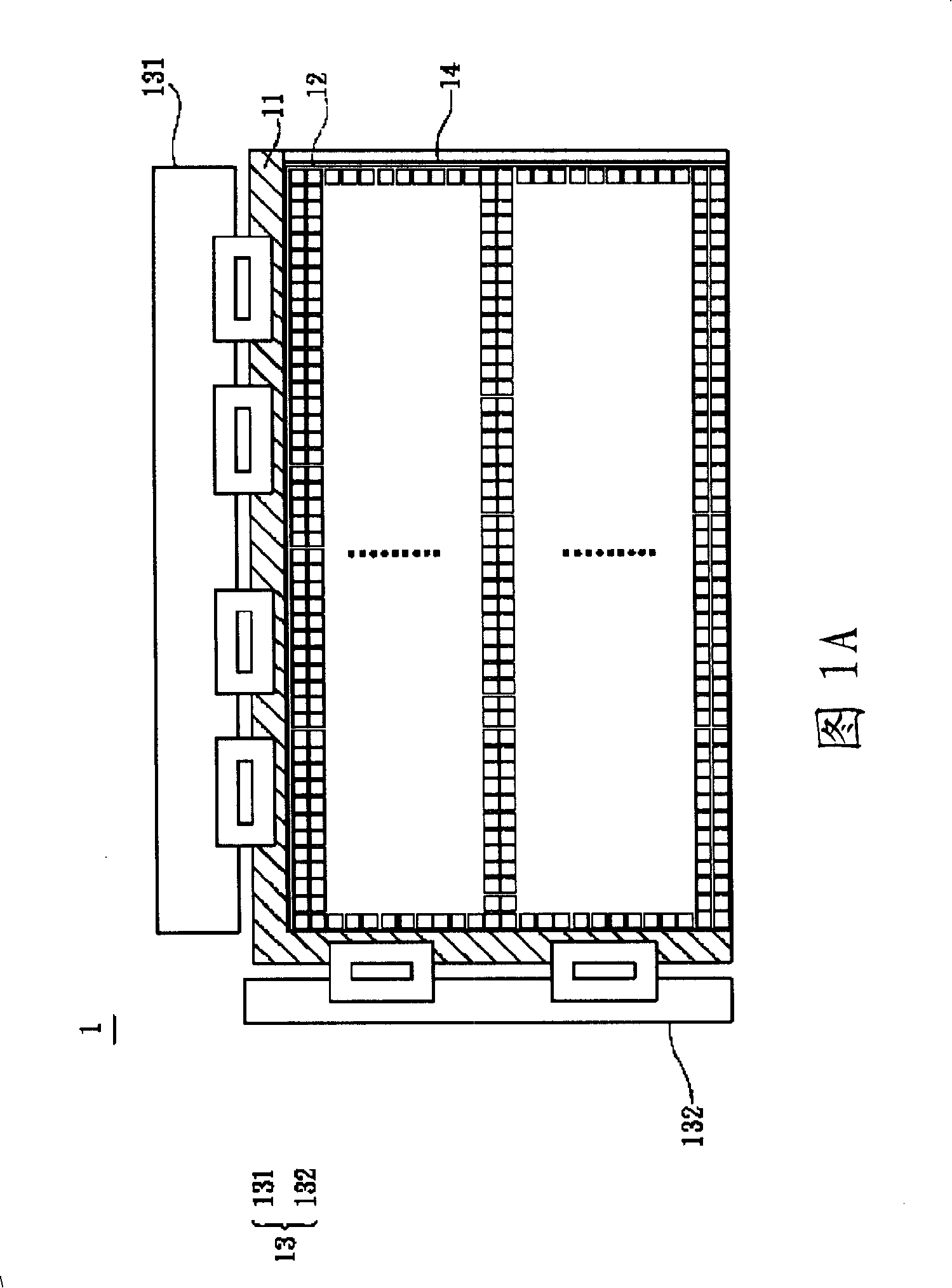
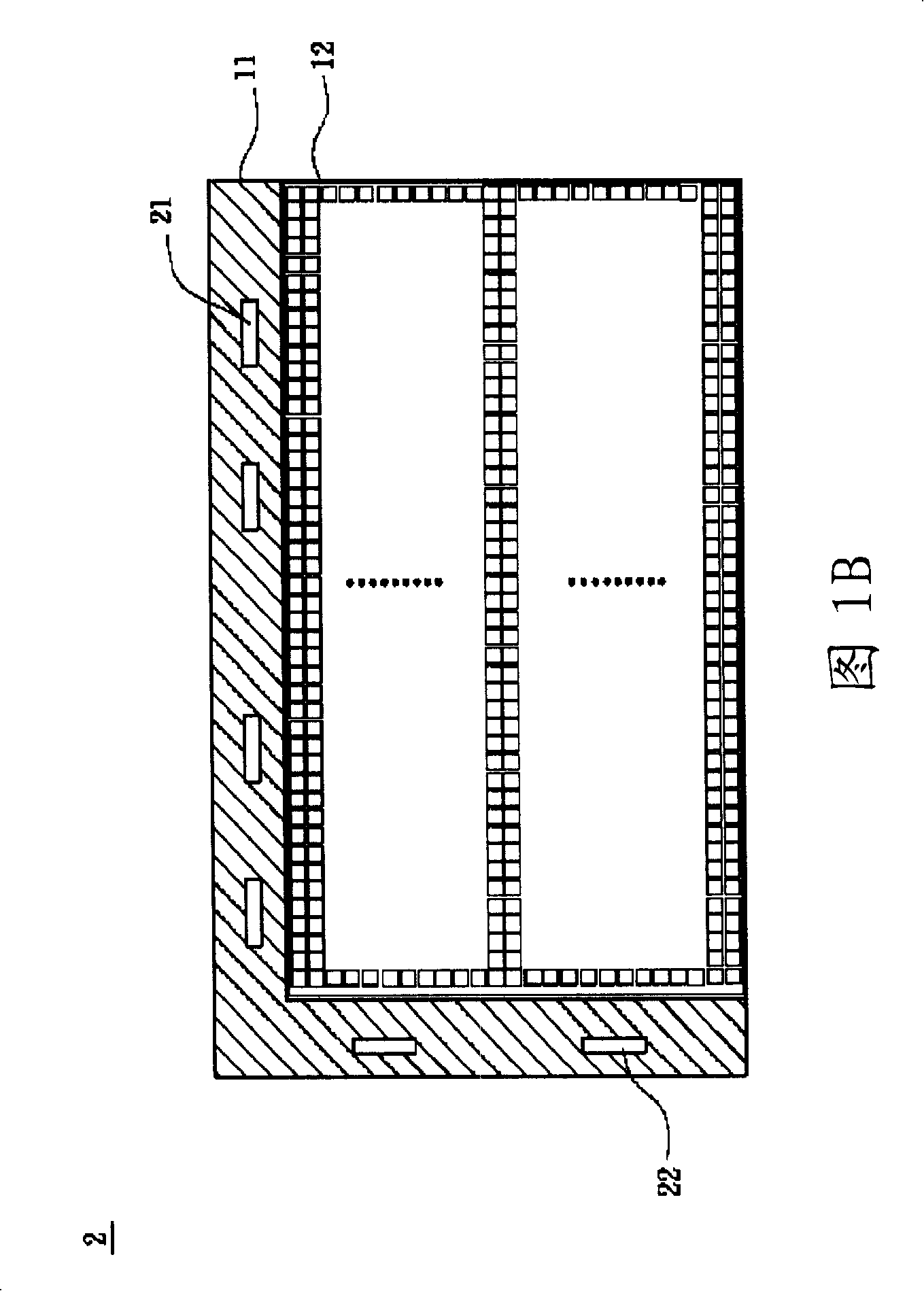
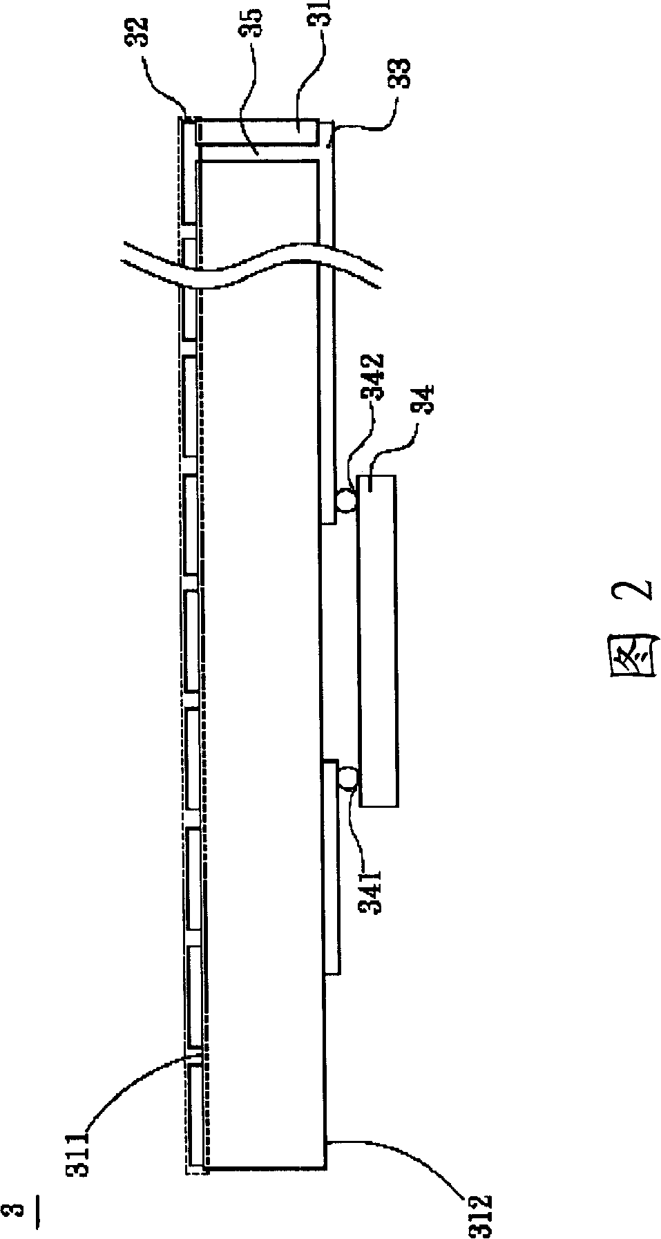
[0065] Please refer to FIG. 2 , a pixel array module 3 according to a preferred embodiment of the present invention includes a substrate 31 , a pixel electrode array 32 , a patterned conductive layer 33 and a semiconductor circuit unit 34 .

[0066] The substrate 31 has a first surface 311 and a second surface 312 , and the first surface 311 and the second surface 312 are opposite to each other. Wherein, the substrate 31 is a printed circuit board (printed circuitboard, PCB) or a flexible circuit board (flexible printed circuit, FPC). In this embodiment, the substrate 31 is a double-sided printed circuit board as an example. It is a multi-layer printed circui...


PUM


Abstract

The present invention relates to a pixel array module and a flat panel display device. The pixel array module comprises a basal plate, a pixel electrode array, a patterned conductive layer and a semiconductor circuit unit. The basal plate has a first surface and a second surface arranged oppositely to the first surface. The pixel electrode array is arranged on the first surface of the basal plate. The patterned conductive layer is arranged on the second surface of the basal plate and is electrically connected with the pixel electrode array. The semiconductor circuit unit has at least one input end and at least one output end in electrical connection with the patterned conductive layer. The present invention also discloses a flat panel display device. The present invention has the pixel electrode array and the patterned conductive layer arranged respectively on two sides of the basal plate, ensuring that either surface of the basal plate is used completely as a display surface. Therefore, when the present invention is applied to splice type display devices, optimal imaging manifestation can be obtained.

Description

technical field [0001] The present invention relates to a pixel array module and a display device, in particular to a pixel array module and a flat display device suitable for splicing display. Background technique [0002] The development of display technology enables people to easily receive various information through display devices, thus enriching people's life and speeding up the transmission speed of information. [0003] Please refer to FIG. 1A , a general flat panel display device 1 mainly includes a substrate 11 , a pixel array 12 , a driving circuit 13 and a photoelectric display unit 14 . Wherein the driving circuit 13 has a data line driving circuit 131 and a scanning line driving circuit 132, and the photoelectric display unit 14 has a counter electrode opposite to the pixel array 12, and is arranged between the counter electrode and the pixel array 12. optoelectronic display elements. [0004] The driving circuit 13 is electrically connected to the pixel arr...

Claims


Application Information

Patent Timeline
Patent Type & Authority Applications(China)
IPC IPC(8): G02F1/167H01L25/00H01L23/488G09F9/37G09F9/00
CPCH01L2224/16225
Inventor 萨文志
Owner GIGNO TECH CO LTD
Why Eureka
Try Eureka