LCD panel preparation method
A manufacturing method and technology of liquid crystal panels, applied in nonlinear optics, instruments, optics, etc., can solve the problems of large exposed area of wires, affecting the yield of liquid crystal panels, disconnection or bending of wires, etc.
- Summary
- Abstract
- Description
- Claims
- Application Information
AI Technical Summary
Problems solved by technology
Method used
Image

Examples
Embodiment Construction
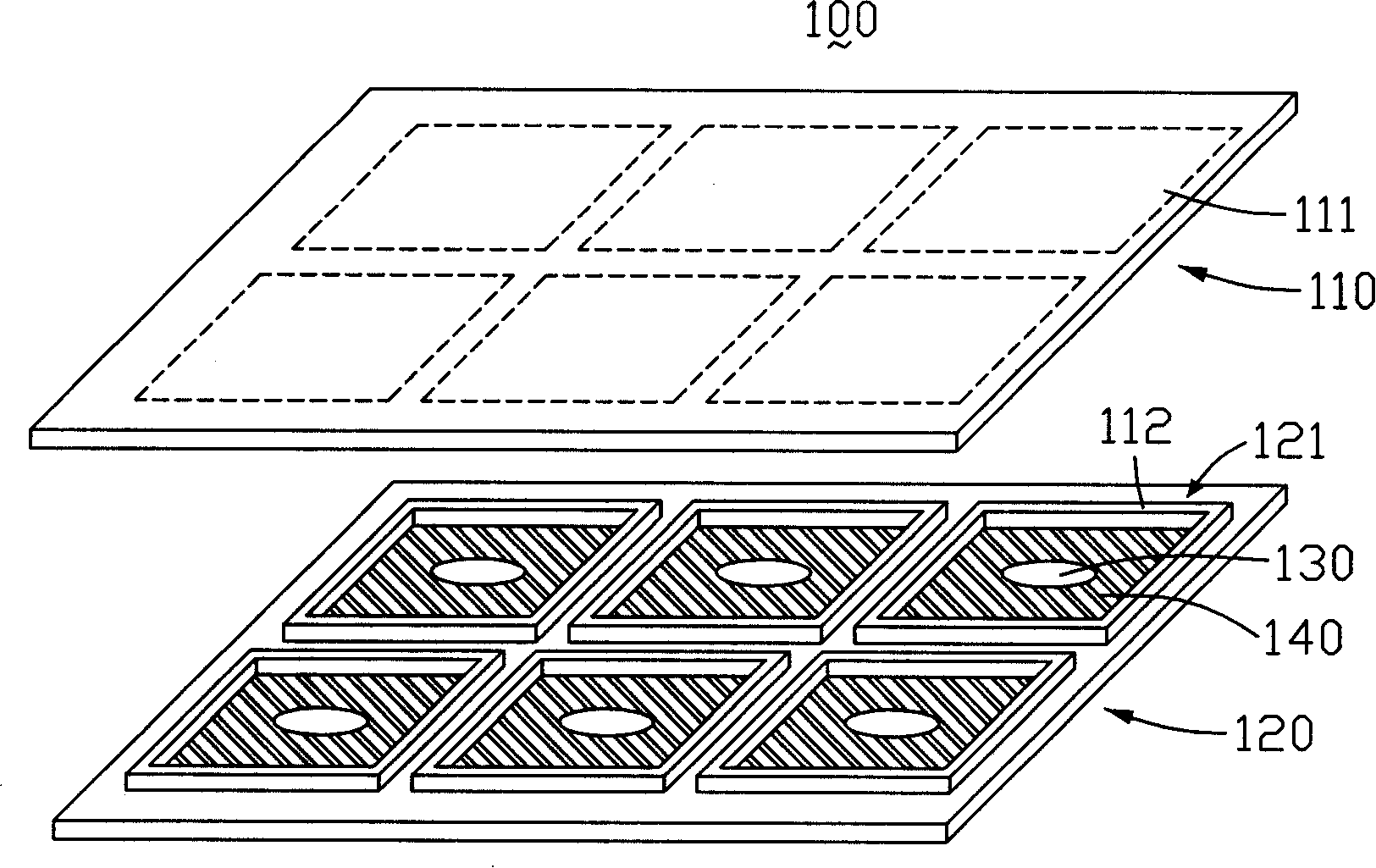
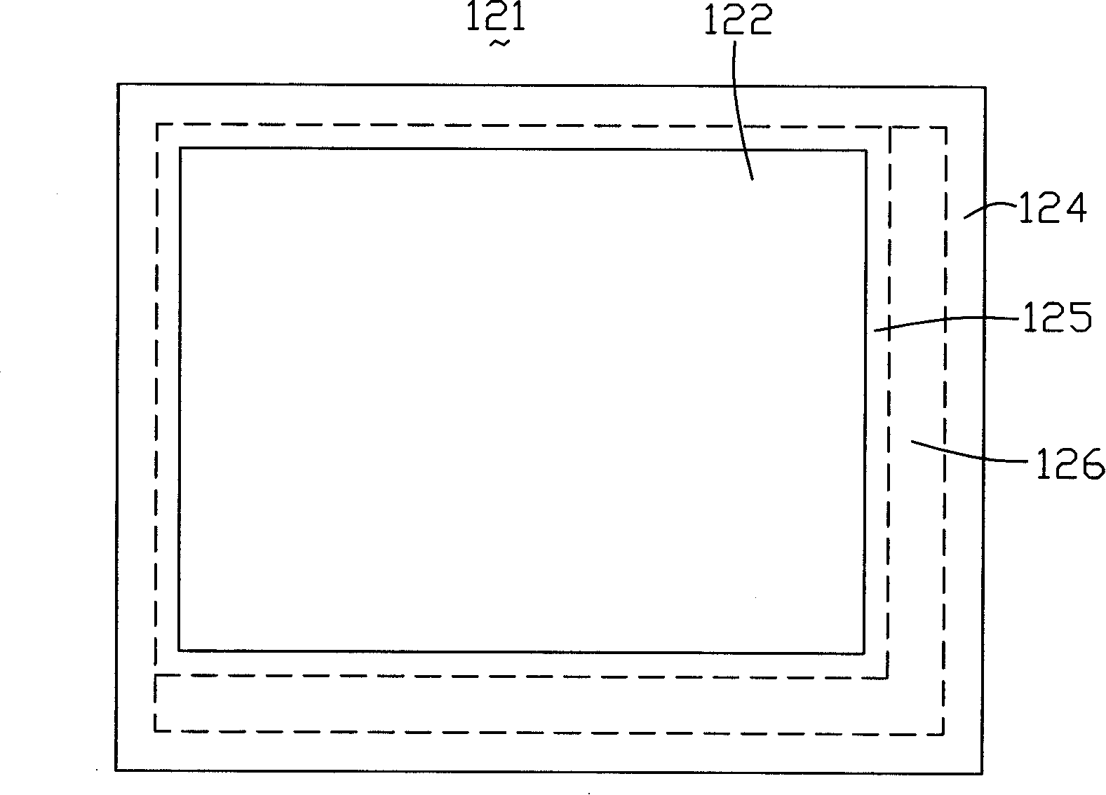
[0032] see Figure 4 , is a schematic structural view of the liquid crystal panel to be manufactured in the present invention. The liquid crystal panel 20 includes a first substrate 210 , a second substrate 220 , a liquid crystal 250 , a frame glue 260 and a driver chip 290 . The second substrate 220 is disposed opposite to the first substrate 210 , and a part of the second substrate 220 extends outward compared with the first substrate 210 . The sealant 260 is interposed between the second substrate 220 and the first substrate 210 , and forms a liquid crystal cell (not shown) with the second substrate 220 and the first substrate 210 . The liquid crystal 250 is arranged in a liquid crystal cell. The driving chip 290 is disposed on an area where the second substrate 220 extends outwards compared with the first substrate 210 .
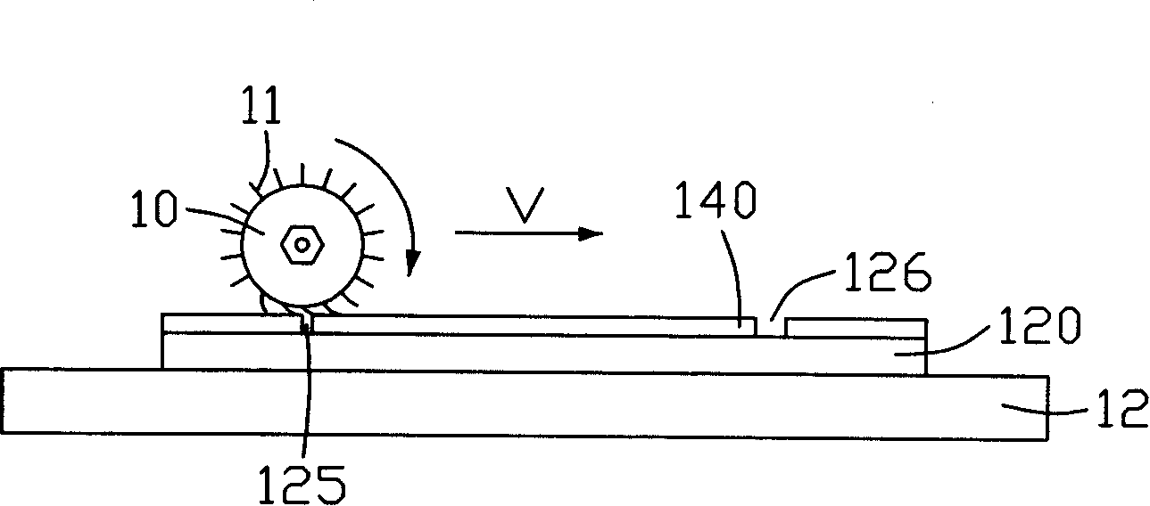
[0033] see Figure 5 , is a flow chart of a preferred embodiment of the liquid crystal panel manufacturing method of the present invention. The spe...
PUM
 Abstract
Description
Claims
Application Information
 - R&D
- Intellectual Property
- Life Sciences
- Materials
- Tech Scout
- Unparalleled Data Quality
- Higher Quality Content
- 60% Fewer Hallucinations
Browse by: Latest US Patents, China's latest patents, Technical Efficacy Thesaurus, Application Domain, Technology Topic, Popular Technical Reports.
© 2025 PatSnap. All rights reserved.Legal|Privacy policy|Modern Slavery Act Transparency Statement|Sitemap|About US| Contact US: help@patsnap.com