Check patentability & draft patents in minutes with Patsnap Eureka AI!

Printed circuit board and element module packaging structure and encapsulation method

A technology of printed circuit board and packaging structure, which is applied in the direction of printed circuit components, printed circuit, printed circuit, etc., which can solve the disadvantages of miniaturization and high integration design of printed circuit board, increased difficulty of printed circuit board wiring, and functional module area Increase and other problems, to save assembly space, simplify the soldering and packaging process, and reduce the size of the module

Inactive Publication Date: 2008-07-02
AIGO DIGITAL TECHNOLOGY CO LTD +1
View PDF0 Cites 7 Cited by
  • Summary
  • Abstract
  • Description
  • Claims
  • Application Information

AI Technical Summary

Problems solved by technology

[0004] The above-mentioned first type of direct welding between printed circuit boards and components is suitable for welding components and printed circuit boards when the integration level is not high. If the integration level of components is high When the packaging components of the components are small, the wiring difficulty of the printed circuit board will increase, and the requirements for the manufacturing process of the printed circuit board will also be improved, and the cost will increase; the above-mentioned second printed circuit board and functional module Direct packaging integrates core or key components into functional modules, which reduces the difficulty of welding with printed circuit boards to a certain extent. This leads to an increase in the wiring difficulty of the printed circuit board, which is not conducive to the miniaturization and high integration design of the printed circuit board

Method used


Image

  • Printed circuit board and element module packaging structure and encapsulation method
  • Printed circuit board and element module packaging structure and encapsulation method
  • Printed circuit board and element module packaging structure and encapsulation method

Examples


Embodiment Construction

[0026] In order to further explain the technical means and effects adopted by the present invention to achieve the predetermined purpose, the specific implementation, structural features and effects of the packaging structure and packaging method of the printed circuit board and component module of the present invention will be described in detail below in conjunction with the accompanying drawings and embodiments. described as follows.

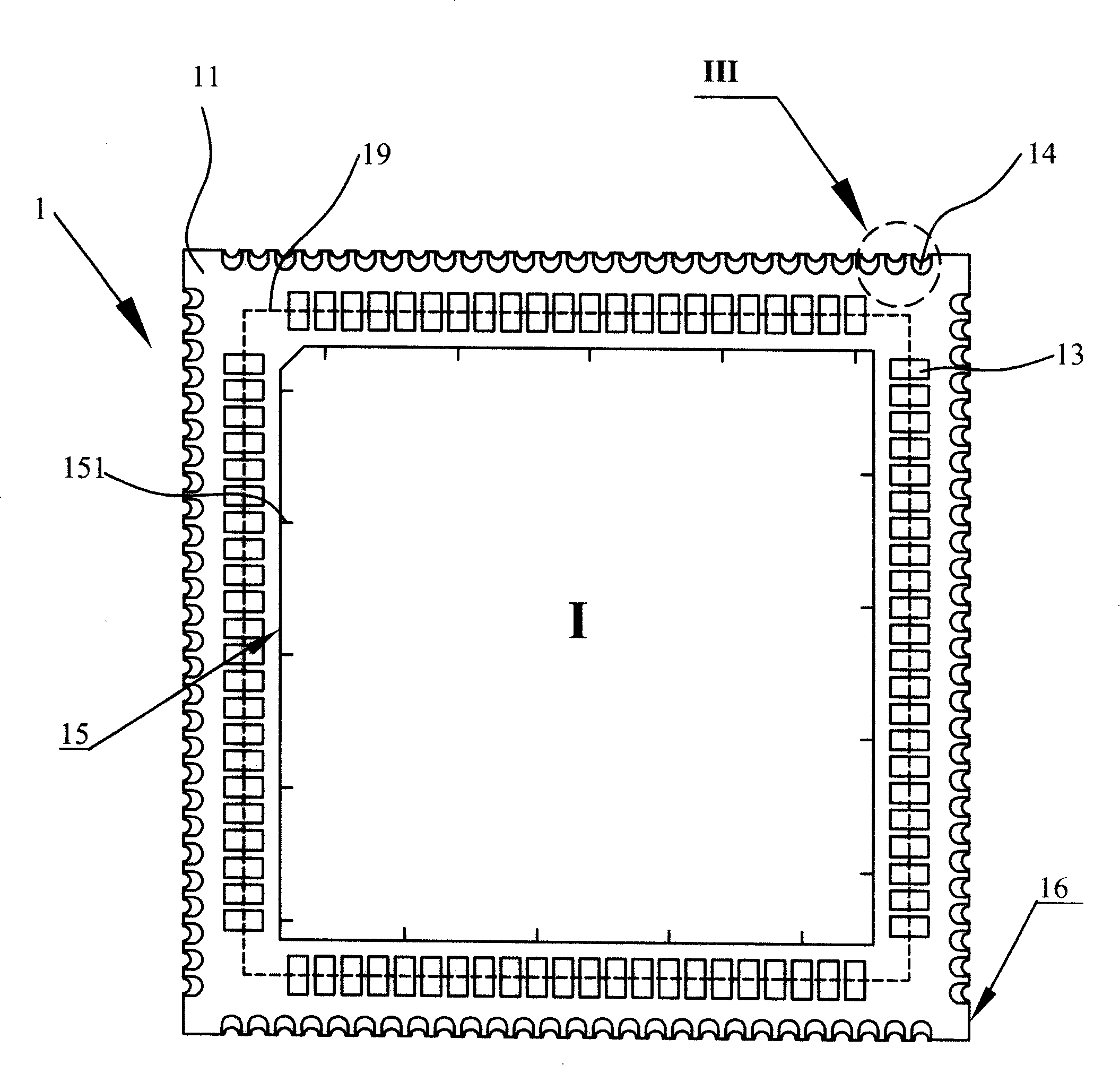
[0027] Please refer to FIG. 11 , the packaging structure 3 of the printed circuit board and the component module of the present invention includes the component module 1 and the printed circuit board 2 . In a specific embodiment, the core and key components that can realize certain functions are designed as integrated component modules, such as, the image receiving and processing modules are integrated and designed as image component modules, and the optical signal processing components are integrated and designed Component modules for optica...


PUM


Abstract

The invention discloses an encapsulation structure of a printed circuit board and an element module, which consists of a base board of the printed circuit board and the element module. A through hole corresponding with the element module is arranged in the base board of the printed circuit board; the element module comprises a first and a second encapsulation surface; a first and a second encapsulation endpoint is positioned on the side edge of the first encapsulation surface; the element module is arranged on the through hole of the printed circuit board correspondingly; the first and second encapsulation endpoints of the first encapsulation surface in the element module are electrically contacted and encapsulated with the first and second welding spots on the first bearing surface of the printing circuit plate. Through welding and encapsulating respectively to the first and second encapsulation endpoints led by the first bearing surface of the element module, the invention reduces the wiring difficulty of the printed circuit board, simplifies the welding and encapsulating technology of the printing circuit plate. Furthermore, the element module can adopt the design of placing devices on double side which is conducive to reducing the assembling size, saving assembling space.

Description

【Technical field】 [0001] The invention relates to a packaging structure of a printed circuit board, in particular to a packaging structure of a printed circuit board and an element module and a packaging method thereof, which simplify the packaging process and reduce the difficulty of packaging. 【Background technique】 [0002] The development of electronic technology has made the integration of components on the circuit board higher and higher, so that the soldering and packaging process of the printed circuit board also needs to adapt to the development of high integration of components. [0003] The main methods of welding traditional printed circuit boards and components include: the first method is to directly solder the components to the printed circuit board; the second method is to integrate the core components into functional modules, and the components of the functional modules The relevant pins are led out from the periphery and welded with the printed circuit boar...

Claims


Application Information

Patent Timeline
IPC IPC(8): H01L23/488H01L23/482H01L23/498H01L21/60H01L21/48H05K1/02H05K1/18H05K3/00H05K3/34
CPCH05K1/141H01L2924/0002H01L25/0657H01L23/49805H05K2201/09181H05K1/182H01L23/49838H05K2203/1572H05K3/3442H01L2225/06551
Inventor 邓国源曾巨航
Owner AIGO DIGITAL TECHNOLOGY CO LTD
Features
  • R&D
  • Intellectual Property
  • Life Sciences
  • Materials
  • Tech Scout
  • Unparalleled Data Quality
  • Higher Quality Content
  • 60% Fewer Hallucinations
Learn More