Packaged memory chip and embedded device comprising same

A technology for embedded devices and memory chips, applied in semiconductor devices, electrical components, circuits, etc., can solve the problems of not being too small in the area of ​​memory chips, difficult to wire, and large area of ​​memory chips, and to reduce the difficulty of wire bonding, The effect of reducing the number of pins and reducing the area

Active Publication Date: 2012-12-12
GIGADEVICE SEMICON (BEIJING) INC
View PDF3 Cites 10 Cited by
  • Summary
  • Abstract
  • Description
  • Claims
  • Application Information

AI Technical Summary

Problems solved by technology

It can be seen that using Parallel NOR FLASH and parallel PSRAM for chip packaging, the number of balls is large, and it is difficult to wire, which also causes the area of ​​the packaged memory chip to not be too small
In addition, since the area of ​​Parallel NOR FLASH is much larger than that of parallel PSRAM, the area of ​​this memory chip is mainly determined by Parallel NOR FLASH, and since the area of ​​Parallel NOR FLASH is relatively large, the area of ​​the packaged memory chip bigger

Method used


Image

  • Packaged memory chip and embedded device comprising same
  • Packaged memory chip and embedded device comprising same
  • Packaged memory chip and embedded device comprising same

Examples


Embodiment Construction

[0029] The principles and features of the present invention are described below in conjunction with the accompanying drawings, and the examples given are only used to explain the present invention, and are not intended to limit the scope of the present invention.

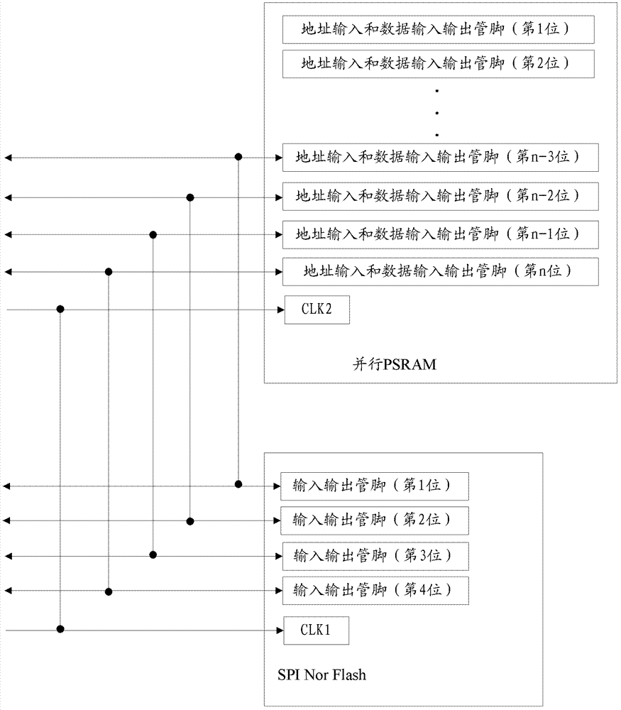
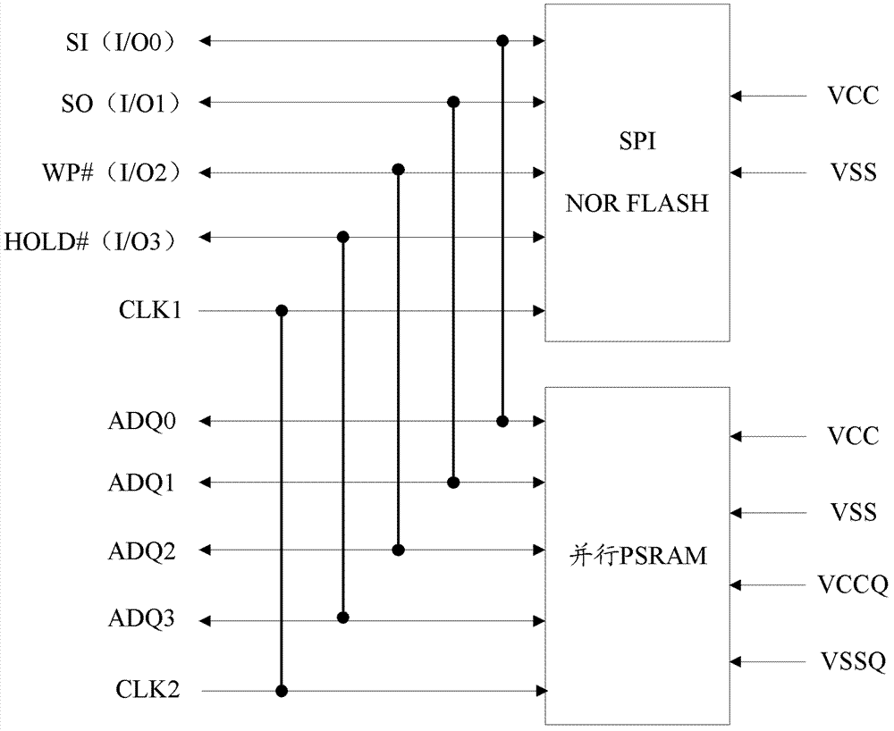
[0030] figure 1 A structural diagram of a packaged memory chip provided by the present invention. Such as figure 1 As shown, the memory chip includes: packaged serial non-volatile flash memory (SPI NOR FLASH) and parallel pseudo static random access memory (PSRAM); SPI NOR FLASH includes a clock input pin (CLK1) and four input and output pins ;Parallel PSRAM includes clock input pin (CLK2), more than four address input and data input and output pins; among them, the four input and output pins of SPI NOR FLASH and any four address input and data input of parallel PSRAM The output pins are connected respectively, and CLK1 is connected with CLK2.

[0031] Here, the SPI NOR FLASH is a serial non-volatile flash memory...


PUM


Abstract

The invention relates to a packaged memory chip and an embedded device comprising the same. The memory chip comprises a packaged SPI (serial peripheral interface) NOR FLASH and a parallel PSRAM (pseudo static random access memory); the SPI NOR FLASH comprises a clock input pin and four input and output pins; the parallel PSRAM comprises a clock input pin CLK2 and more than four address input and data input and output pins; and the four input and output pins of the SPI NOR FLASH are respectively connected with optional four of the address input and data input and output pins of the parallel PSRAM, and the CLK1 is connected with the CLK2. According to the technical scheme, the area of the packaged memory chip can be reduced.

Description

technical field [0001] The invention relates to the technical field of chip packaging, in particular to a packaged memory chip and an embedded device using the memory chip. Background technique [0002] With the increasingly diversified requirements of various portable information devices for memory characteristics, in order to solve the problem of insufficient integration and functions of a single chip, a multi-chip package (Multi Chip Package, which can package several chips in one place) has emerged. MCP) technology has the advantage that two to three chips with different characteristics can be packaged together to form a chip, which can reduce the space occupied by the chip and improve the integration and functional perfection of the chip. Samsung Electronics, Hyundai Electronics, Intel and other global heavyweight integrated circuit manufacturers have recently been optimistic about the market prospect of this type of memory, and have launched related products. [0003]...

Claims


Application Information

Patent Timeline
Patent Type & Authority Applications(China)
IPC IPC(8): H01L27/115
Inventor 龙钢
Owner GIGADEVICE SEMICON (BEIJING) INC
Why Eureka
Try Eureka