Chip carrier with dams

A carrier and chip technology, which is applied in electric solid state devices, semiconductor devices, semiconductor/solid state device components and other directions, and can solve problems such as easy overflow and contamination of solder ball connection pads.

Inactive Publication Date: 2008-07-23
ADVANCED SEMICON ENG INC
View PDF0 Cites 15 Cited by
  • Summary
  • Abstract
  • Description
  • Claims
  • Application Information

AI Technical Summary

Problems solved by technology

[0002] A known substrate has a plurality of bump connection pads and a plurality of solder ball connection pads, usually the bump connection pads and the solder ball connection pads are located on the same plane of the substrate and the bump connection pads are in phase with the solder ball connection pads. Adjacent, due to the current requirements for electronic products to be light, thin and short, the distance between the bump connection pad and the solder ball connection pad is quite small. When the chip is electrically connected to the substrate with bumps and filled with underfill When sealing the bump between the substrate and the chip, the underfill is likely to overflow to the solder ball connection pad and contaminate the adjacent solder ball connection pad, causing the solder ball connection pad to be damaged in subsequent processes. Unable to bond smoothly with solder balls

Method used


Image

  • Chip carrier with dams
  • Chip carrier with dams
  • Chip carrier with dams

Examples


Embodiment Construction

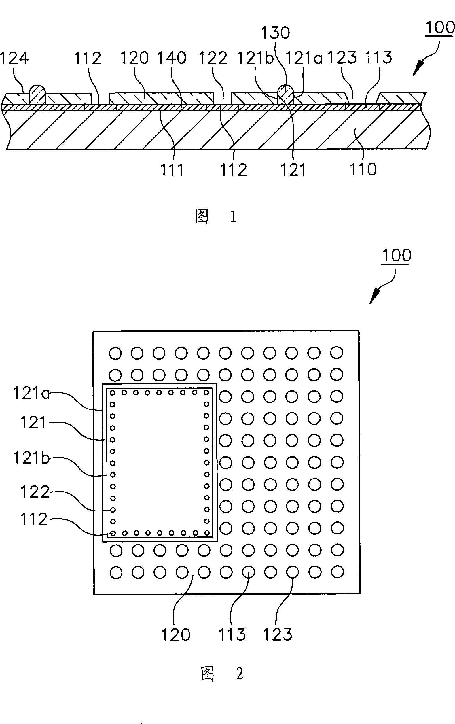
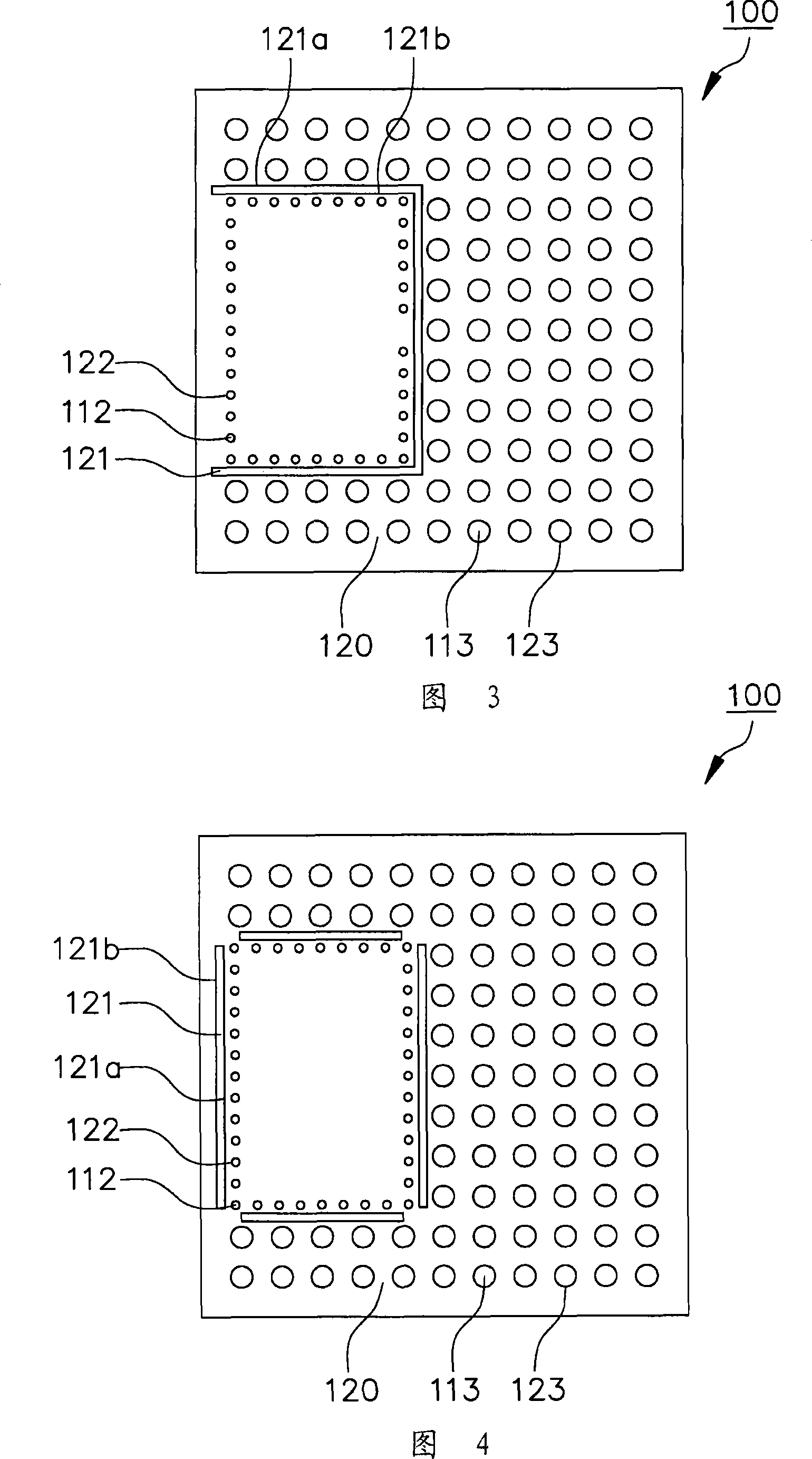
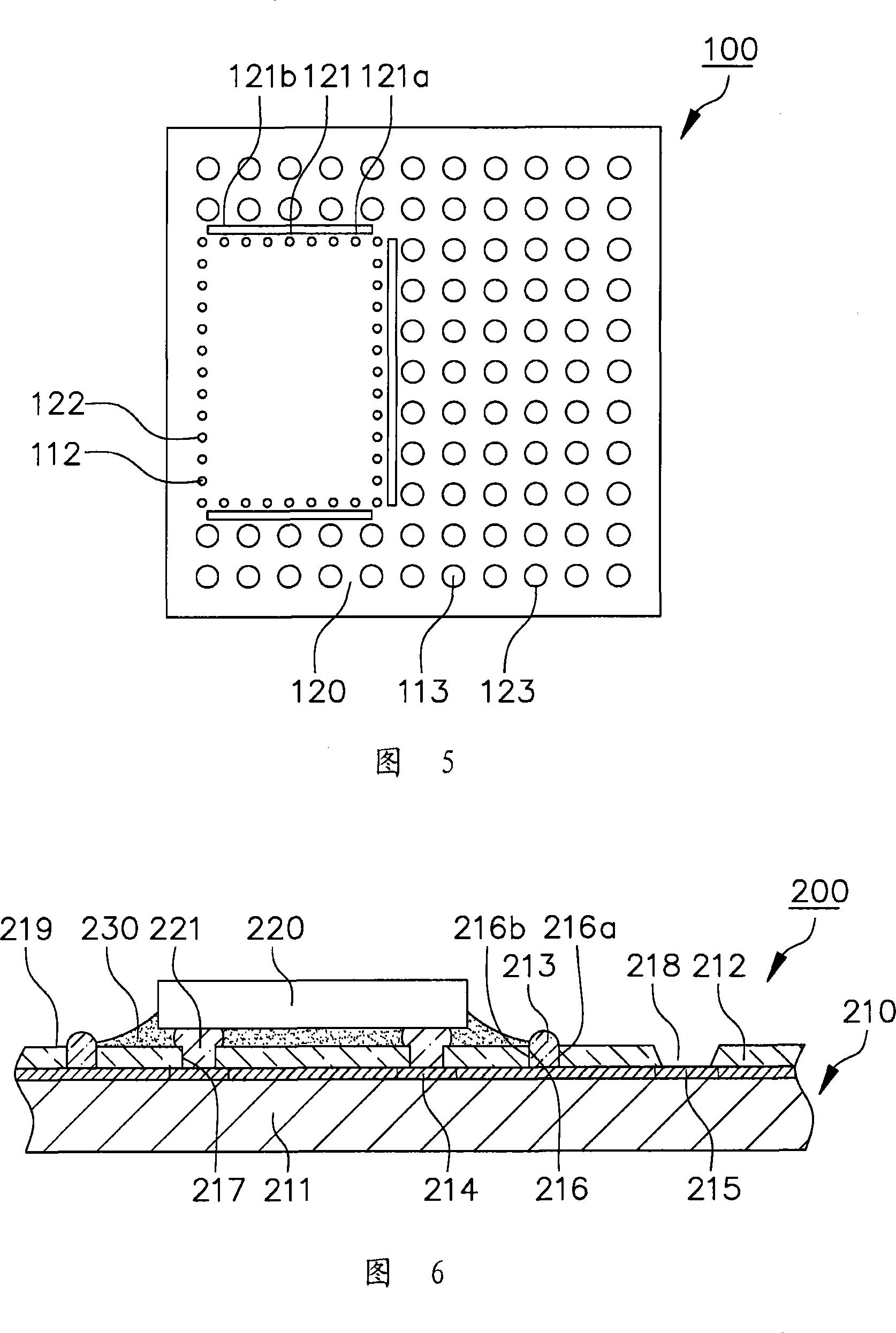
[0027] Please refer to FIG. 1 , according to a specific embodiment of the present invention, a chip carrier 100 with a dam is disclosed, which mainly includes a substrate 110, a protective layer 120 and a dam 130. The substrate 110 can be selected from a chip , chip or circuit board, the substrate 110 has a substrate surface 111, a plurality of first connection pads 112 and a plurality of second connection pads 113, the first connection pads 112 and the second connection pads 113 are formed on the substrate Surface 111, in addition, the chip carrier 100 further includes a circuit layer 140, the circuit layer 140, the first connection pad 112 and the second connection pad 113 can be formed by a metal layer after a patterning step, in this embodiment , the base material 110 is a printed circuit board, the protective layer 120 is a solder mask, such as green paint, the first connection pad 112 is a bump connection pad, and the second connection pad 113 is a solder ball connection ...


PUM


Abstract

The invention discloses a chip carrier with a barrage, which mainly comprises a base material, a protective layer and a barrage. The base material is equipped with a plurality of first connecting pads and second connecting pads, the protective layer is formed on the surface of the base material and is equipped with a dent, a plurality of first openings and second openings, wherein the dent is equipped with a first lateral wall and a second lateral wall, the first openings and the second openings respectively expose the first connecting pads and the second connecting pads. The barrage is formed between the first lateral wall and the second lateral wall of the dent, and projects out of the protective layer. The barrage has the function of preventing the overflow of under fill polluting chip carrier. The barrage is formed in the dent of the protective layer, thereby the width and height of the barrage can be controlled, and the touching area and bond strength of the barrage and the protective layer can be increased to avoid the peeling of the barrage and the protective layer. The invention also discloses a semi-conductor structure.

Description

technical field [0001] The invention relates to a chip carrier, in particular to a chip carrier capable of preventing overflow glue from polluting connection pads. Background technique [0002] A known substrate has a plurality of bump connection pads and a plurality of solder ball connection pads, usually the bump connection pads and the solder ball connection pads are located on the same plane of the substrate and the bump connection pads and the solder ball connection pads are in phase Adjacent, due to the current requirements for electronic products to be light, thin and short, the distance between the bump connection pad and the solder ball connection pad is quite small. When the chip is electrically connected to the substrate with bumps and filled with underfill When sealing the bump between the substrate and the chip, the underfill is likely to overflow to the solder ball connection pad and contaminate the adjacent solder ball connection pad, causing the solder ball c...

Claims


Application Information

Patent Timeline
Patent Type & Authority Applications(China)
IPC IPC(8): H01L23/13H01L23/488
CPCH01L2224/73204
Inventor 陈家庆陈裕文
Owner ADVANCED SEMICON ENG INC
Why Eureka
Try Eureka