Check patentability & draft patents in minutes with Patsnap Eureka AI!

A serial interface flash memory and its design method

A serial interface and memory technology, applied in the field of serial interface flash memory and its design, can solve the problems of limited number of pins and inability to meet the data transmission rate requirements, and achieve the effect of improving the data transmission rate

Active Publication Date: 2008-08-06
GIGADEVICE SEMICON (BEIJING) INC
View PDF0 Cites 8 Cited by
  • Summary
  • Abstract
  • Description
  • Claims
  • Application Information

AI Technical Summary

Problems solved by technology

However, for the standard serial interface flash memory, the number of pins is limited, and the current pin reuse has reached the limit
Even if the scheme of high clock frequency and pin multiplexing is adopted at the same time, it cannot meet the industry's increasingly high data transmission rate requirements for serial interface flash memory.

Method used


Image

  • A serial interface flash memory and its design method
  • A serial interface flash memory and its design method
  • A serial interface flash memory and its design method

Examples


Embodiment Construction

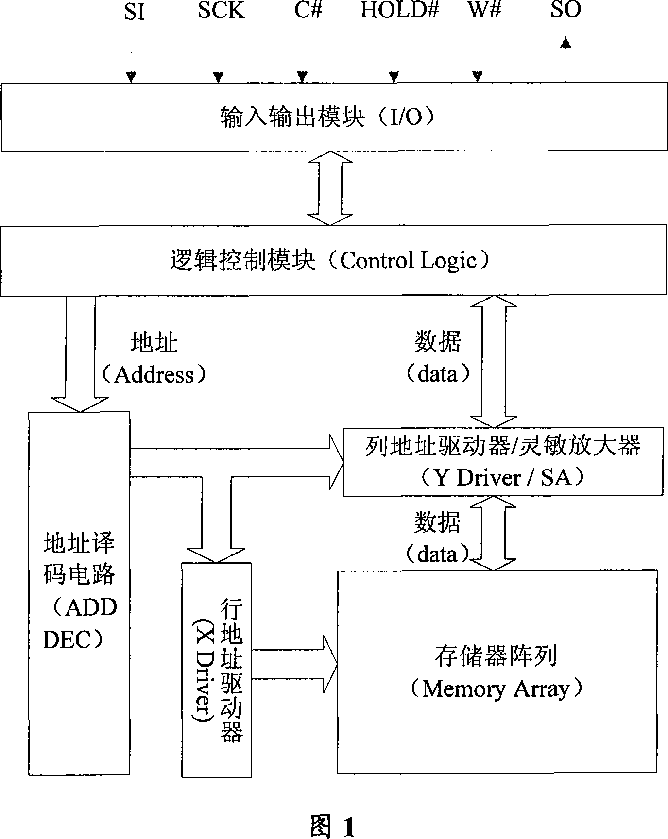
[0026] Serial interface flash memory uses clock signals to control various operations such as reading, writing, and erasing. A clock signal is a signal that changes between "1" (high level) and "0" (low level) at a specific frequency, so the clock signal changes from "0" to "1" (rising edge), It also changes from "1" to "0" (falling edge), with one clock cycle between two rising edges or between two falling edges.

[0027] The key point of the present invention is: using the rising edge and the falling edge of the external clock signal to operate the serial interface flash memory once, that is, to realize that the memory is operated twice in one clock cycle. For example, when reading data from the memory, one read operation is performed on the rising edge and the falling edge of the clock. Compared with only one read operation in one clock cycle, the transmission rate of the read data is doubled, that is, double the data transmission rate. Data transfer rate (Double Data Rate...


PUM


Abstract

The invention discloses a serial interface flash memory and a designing method thereof. The serial interface flash memory comprises a logic control module which comprises a clock conversion circuit; the clock conversion circuit is used for sampling the rising edge and the falling edge of an external clock signal; a sampling result as an internal clock signal is output. Furthermore, the logic control module also comprises a mode control unit which is used for receiving a mode command; the clock conversion circuit is enabled or forbidden according to the mode command. According to the invention, the data transmission speed of the serial interface flash memory can be effectively improved.

Description

technical field [0001] The present invention relates to a flash memory, in particular to a serial interface flash memory and a design method thereof. Background technique [0002] Serial interface flash memory is a widely used data storage device with the characteristics of non-volatile storage and serial transmission. Due to the use of serial data transmission, the serial interface flash memory has only one data input pin, one data output pin and several other functional pins. The advantage of particularly low is widely favored by system designers. However, because all read and write instructions, addresses and stored data are serial input and output, the slow data transmission rate has become the biggest disadvantage of serial interface flash memory, and improving its data transmission rate has become the industry's most important problem in serial interface flash memory. urgent need for memory. [0003] The serial interface flash memory uses the clock signal input by t...

Claims


Application Information

Patent Timeline
Patent Type & Authority Applications(China)
IPC IPC(8): G11C7/10
Inventor 朱一明胡洪
Owner GIGADEVICE SEMICON (BEIJING) INC
Features
  • R&D
  • Intellectual Property
  • Life Sciences
  • Materials
  • Tech Scout
  • Unparalleled Data Quality
  • Higher Quality Content
  • 60% Fewer Hallucinations
Learn More